Spintronics Research in Semiconductor Nanowires
Laboratory on Nanowires X Spin Devices
Professor:AKABORI Masashi
E-mail:
[Research areas]
Epitaxial growth, Nanostructures, Spintronics
[Keywords]
Semiconductors, Magnetic metals, Nanofabrication, Electrical measurement, Magnetic field, Low temperature
Skills and background we are looking for in prospective students
Our laboratory is experimentally studying solid state materials and devices. Therefore, students who like to handle them will be matched with us. The students should better have physics background especially electromagnetism and quantum mechanics, and basic background of solid state physics including semiconductor physics, chemistry, programing, etc. The backgrounds will be helpful for studying in our laboratory.
What you can expect to learn in this laboratory
In our laboratory, the students will operate various equipment. The operation is considered based on principles and logical thinking. Therefore, with understanding and performing the operations, the students will learn the principles and logical thinking way. Also since in experimental studies there are lots of troubles/problems, sometimes it is difficult to obtain expected results and scheduled progress as well. However, by analyzing the troubles/problems and the results with cooperation with other members, the students will pay their own efforts to obtain more good results, and finally will learn problem discovering ability and problem solving ability.
【Job category of graduates】
Electronic Devices/Materials, Electrical/Precision Machinery, Communication/Information Technology
Research outline
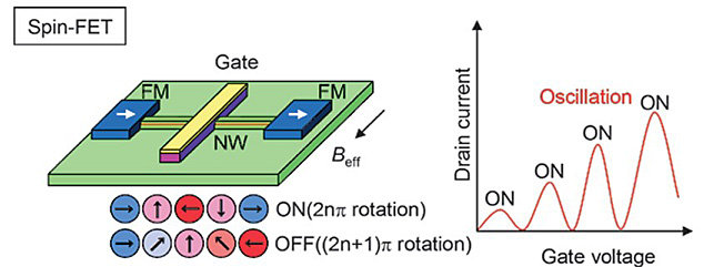
Fig. 1.Spin-FET
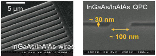
Fig. 2. Wire channel and point
contact by top-down methods
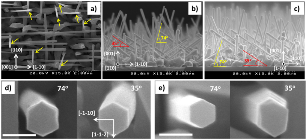
Fig. 3. NWs by bottom-up methods
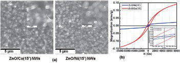
Fig. 4. Electrochemical deposited core/shell NWs
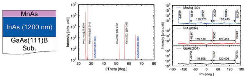
Fig. 5 MnAs/InAs hybrid structure
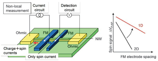
Fig. 6. Non-local measurement
The information technology supported by the electronics is based on controlling electric charge. The spintronics is controlling not only electric charge but also spin direction for the future information technology. In the IEEE International Roadmap for Devices and Systems (IRDS), the spintronic devices are ranked as important next-generation devices. The most typical spintronic device using a semiconductor (SC) is spin field-effect transistor (spin-FET), which consists of a SC channel having large spin-orbit coupling (InAs, InGaAs, InSb, InGaSb etc.) and ferromagnetic metal (FM) electrodes (Fig. 1). By using SC nanowire (NW) as the channel, spin relaxation caused by the spin-orbit coupling and elastic scattering is expected to be suppressed in the spin-FET. According to the background, we investigate NW-FM hybrid structures for spintronic applications.
(1) Formation of SC NW structures
We investigate top-down and bottom-up formation of SC NWs. In the top-down method, we process high-quality SC heterojunctions by using electron beam lithography and etching technique (Fig. 2). In this case, the challenges for coherent spin transport are optimization of the edge shape and suppression of the etching damage. In the bottom-up method, we use molecular beam epitaxy on masked substrates (Fig. 3). In this case, it is difficult to utilize heterojunctions, however, it is possible to achieve fine shape and size of NWs by optimized growth conditions.
(2) Formation of SC/FM hybrid structures
We also investigate electrochemical process of SC (ZnO) / FM (Ni or Co) core/shell NW formation (Fig. 4) and molecular beam epitaxial growth of SC (InAs) / FM (MnAs) hybrid structure formation (Fig. 5). In these methods, continuous interface formation between SC and FM is possible. Therefore, it is also expected that spin injection efficiency from FM to SC becomes higher.
(3) Electrical characterization and analysis
We also carry out electrical characterization and analysis of fabricated NW-FM hybrid structures at low temperatures under magnetic fields by using cryostats with superconducting magnets. By non-local resistance measurements under in-plane magnetic fields (Fig. 6), we can obtain the information of spin injection, transport, and detection. Our final aim is the fabrication of spin-FETs which have not been realized yet in the world.
Key publications
- V. T. Pham, Md. T. Islam, S. Komatsu, M. Akabori: "Temperature dependence of magnetic switching and spin valve behaviors in MnAs/InAs/MnAs double heterostructure on GaAs(111)B" Ceramics International, in press.
- S. Komatsu, M. Akabori: "Enhancement of thermal stability of Zeeman-type spinpolarizer using 1DEG channel and gate-controlled resonant tunneling" Jpn. J. Appl. Phys., Vol.64, pp. 10SP23-1-7 (2025).
- J. Ferdousy, Md. F. Kabir, S. Komatsu, M. Akabori: "Effect of post-deposition annealing atmosphere on ECR-sputtered Fe3O4 thin films and micromagnet fabrication" Jpn. J. Appl. Phys., Vol. 64, pp. 09SP16-1-5 (2025).
Equipment
Common-use deposition system (Molecular Beam Epitaxy, Atomic Layer Deposition, Evaporation, Sputter)
Common-use fabrication system (Electron Beam Lithography, Gas Field Ion Source Focus Ion Beam, Reactive Ion Etching)
Common-use measurement system (Device Analyzer, Hall Effect Measurement System, Magnetic Property Measurement System) Electrochemical deposition system
Lock-in measurement system
Super conducting magnet system
Teaching policy
In our laboratory, we carry out experimental study from formation to characterization/analysis of materials/devices using various equipment. The students are divided into teams by topics, and are asked to have daily team meeting. The staffs join weekly laboratory meeting to grow up communication/presentation/judging skill. Also in the meeting, reading a book and/or paper is carried out to grow up basic scholastic ability and to increase professional knowledge on solid state physics.
[Website] URL : https://www.jaist-akabori-lab.com/