Nanoscale Visualization of Lithium-Ion Battery Dynamics: Integrating Data Science and Electron Microscopy
Laboratory on Microscopic Nano-Characterization
Senior Lecturer:ASO Kohei
E-mail:
[Research areas]
AI-driven nanoscale analysis of materials
[Keywords]
lithium-ion batteries, solid-state physics, nanomaterials, nanoscale measurement, materials characterization, data science, electron microscopy
Skills and background we are looking for in prospective students
We welcome students who are committed and persistent in their research, self-driven, hands-on, and able to collaborate with others. A positive attitude toward daily research is encouraged. Interest in electron microscopy, data science, solid-state physics is a plus, but prior specialized knowledge is not required.
What you can expect to learn in this laboratory
You will develop cross-disciplinary skills for nanoscale characterization of functional materials. You will learn to interpret scanning transmission electron microscopy (STEM) images and electron diffraction patterns, choose and test appropriate analysis methods, and draw valid conclusions linked to crystal structures and materials properties. You will also gain practical STEM skills, Python-based data analysis (image processing, computation, and visualization), and training in literature review, scientific writing/figures, presentations, and discussion.
【Job category of graduates】
Electrical and materials manufacturers, materials analysis companies, university researchers, and technical staff
Research outline
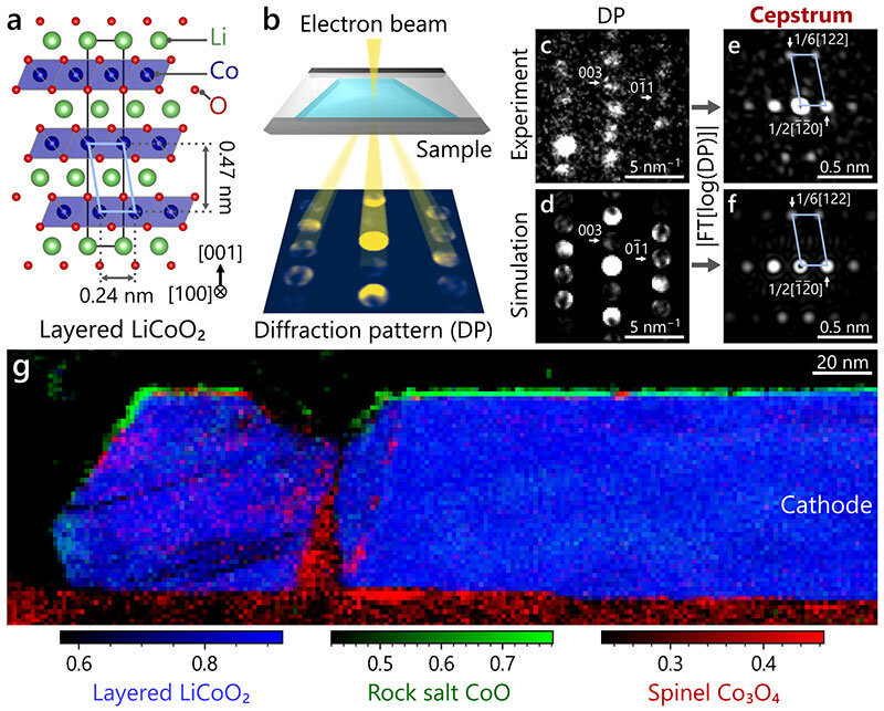
Figure 1: a. Layered cathode (LiCoO2) structure model. b. SNED schematic. Electron diffraction patterns: (c) experiment, (d) simulation. Cepstra from (e) experiment, (f) simulation; bright spots away from the center originate from the crystal structure. (g) Crystal-structure map (blue: layered; green: rocksalt; red: spinel; intensity indicates contribution).
We develop methods that integrate data science and electron microscopy to reveal nanoscale material states that govern device performance. Examples of our research topics include:
- Dynamic nanoscale analysis of all-solid-state lithium-ion battery materials
- Development of nanoscale methods to visualize crystal structures and ion transport
- Atomic-scale imaging of 2D materials and AI-driven quantitative analysis of defects and strain
Below, we briefly introduce part of topic 2.
Visualizing Crystal Structures at the Nanoscale
Lithium-ion batteries (LIBs) are essential energy-storage devices in modern life. Layered materials are widely used as cathodes (Fig. 1a). Understanding nanoscale structural changes in LIB cathodes is increasingly important.
We focus on scanning nanobeam electron diffraction (SNED), a STEM-based technique (Fig. 1b). In SNED, an electron probe is narrowed to approximately 1 nm and scanned across the sample to record diffraction patterns at each position. In practice, diffraction patterns include contributions from sample thickness and local tilts, which can obscure the structural information of interest (Fig. 1c,d). To address this, we analyze cepstra obtained by taking the logarithm of diffraction intensities followed by a Fourier transform. This cepstral approach enhances components related to crystal structures, enabling direct comparison between experiments and simulations (Fig. 1e,f).
Using a crystal-structure map (Fig. 1g), we found that most of the cathode retained the original layered structure. In contrast, within about 3 nm from the electrolyte/cathode interface, we identified spinel and rocksalt structures that are associated with performance degradation. Our method achieves both high spatial resolution (~1 nm) and a wide field of view (~300 nm × 300 nm), while reducing beam-induced damage during observation.
We are now extending this approach to visualize ion transport and track the dynamic behavior of all-solid-state LIBs. Our goal is to generate insights to support LIB material design and synthesis.
Key publications
- K. Aso, T. Kakeya, T. Tsuchida, H. Ito, S. Asano, K. Watanabe, K. Mitsuishi, K. Kimoto, K. Shinoda, T. Masuda, M. Hirayama, and Y. Oshima, “Low-Dose Nanoscale Visualization of Crystal Phases in Epitaxial Cathodes via Cepstral Matching of Scanning Nanobeam Electron Diffraction”, Nano Letters 25 (2025) 15840
- K. Aso, K. Higashimine, M. Miyata, H. Kamio, and Y. Oshima, “Three-dimensional atomic-scale characterization of titanium oxyhydroxide nanoparticles by data-driven lattice correlation analysis”, Communications Chemistry 8 (2025) 122
- K. Aso and Y. Oshima, “Precise positional alignment of atom-resolved HAADF images of heteroepitaxial interface with low signal-to-noise ratio”, Microscopy 74 (2025) 57
Equipment
Scanning transmission electron microscope, workstation PC, scanning electron microscope with focused ion beam, specialized holder for electron microscopy, electrochemical measurement apparatus, and glove box.
Teaching policy
Research topics are set through discussion, taking each student’s interests into account. We hold one-on-one meetings about once a week in an open and approachable atmosphere. Experiments are often conducted with external collaborators, and students gain experience in advancing collaborative research while taking ownership of their work. In lab meetings, students present paper reviews and research updates, and we use Q&A sessions to identify and correct gaps in understanding. We encourage the use of generative AI with careful source checking, proper citation, and clear author responsibility. Our goal is to produce publishable research outcomes. Through close collaboration with the supervisor, students work on advanced research projects, build strong expertise, and graduate with a high level of professionalism.
[Website] URL : https://www.jaist-oshima-labo.com/english/