Creation of electronic films and electron devices by your own energy-saving technique
*This Lab. is not accepting new student.HORITA Laboratory
Professor:HORITA Susumu
E-mail:
[Research areas]
Electron devices, Electronic materials
[Keywords]
thin film, low-temperature process, silicon-based materials, crystallization, semiconductor, insulator, cellulous nanopaper, environmentally friendly materials
Skills and background we are looking for in prospective students
For study on electronic materials and electron devices, you need lots of knowledge about not only physics but also other ones, e.g., chemistry. But, they are not always deep for beginners. That is, the minimum requirement for it is basic and high school level about physics, mathematics, and chemistry at the start of your study. Additionally, if you like deeply thinking, it would be much helpful for improvement of your research work.
What you can expect to learn in this laboratory
For research contributing to society and industry, persistent thinking ability and consistent effort are absolutely necessary. Through researching on energy-save and low-temperature process for electronic material films, you can get knowledge and technique about thin-film formation, device fabrication, material property evaluation, and so on. In due course, you will surely feel much improvement of your research ability from the beginning.
【Job category of graduates】
Manufacture, development and research work in company or researcher in academic position.
Research outline
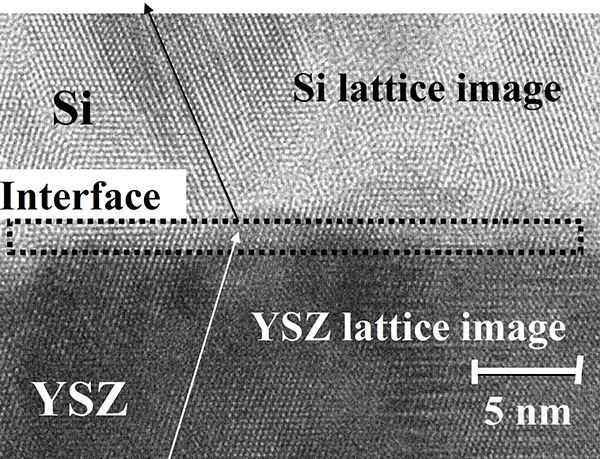
Fig. 1 TEM image (at 430 ℃).
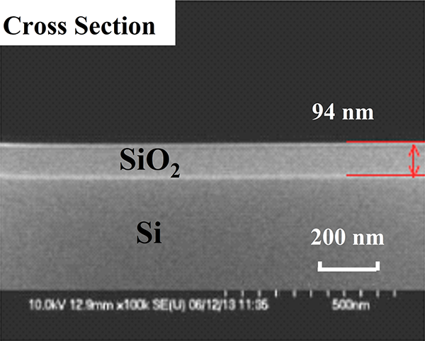
Fig. 2 SEM image (at 200 ℃).
Electron devices, e.g., transistors, are fabricated generally at ≥ 600℃, which is much high temperature, compared with our daily life. Our laboratory tries to form thin films of silicon (Si)-based semiconductor and insulator oxide, e.g., SiO2 at ≲ 200 ℃, which are environmentally friendly materials, and ultimately aims to fabricate transistors on papers. As a result, we can contribute to energy and natural source savings, and environmental preservation.
1) Low-temperature formation of polycrystalline Si film by crystallization-induction layer and laser beam
Because surface of non-expensive substrates like glass has no crystallographic information, deposited films on them at low temperature become amorphous or defective polycrystalline with poor quality. Therefore, we try a following new technique. We deposit a crystalline insulation layer of yttria-stabilized zirconia (YSZ) on the substrate prior to Si film deposition. According to the YSZ crystallographic information, crystallization of a deposited Si film can be induced at lower temperature. Figure 1 shows that crystal growth of the Si film occurs from the YSZ interface. So, we can say that the YSZ layer enhances crystallization of Si film. Now, we try to use a pulsed laser for room-temperature crystallization of Si film.
2) Low-temperature formation of SiO2 film by silicone oil and ozone gas
Using silicon oil used as one of lotion materials and environment- friendly ozone(O3), we deposit SiO2 thin films. The films are produced from thermal chemical reaction at ≲ 200℃ between the oil vapor and O3 gas. Figure 2 shows the secondary electron micrograph of cross section of a silicon oxide film deposited on a Si substrate at 200℃. From this, we can see formation of a flat and 100-nm-thick Si oxide film. At present, we try to remove some amount of Si-OH bonds contained in an as-deposited film at ≲ 200℃ because Si-OH bonds degrade markedly insulation quality.
3) Fabrication of transistors on cellulous nanopaper
Figure 3(a) shows a photograph of comparison between a cellulous nanopaper (CNP) which is by co-researcher Prof. Nogi and a normal white paper, and Fig. 3(b) is a schematic drawing of Si thin-film transistor (TFT) on CNP. CNP has much smooth surface, i.e., a few nm roughness, compared with a normal paper with µm order one. This is because CNP is consisted of nm-order plant cellulous fiber, which is main component of paper while normal paper is µm-order. We will try to make TFT on the extremely smooth surface of CNP. It can be expected that TFT on CNP is disposable device and return to the soil because CNP is made of natural source of cellulous and Si-TFT is mainly made from stone components.
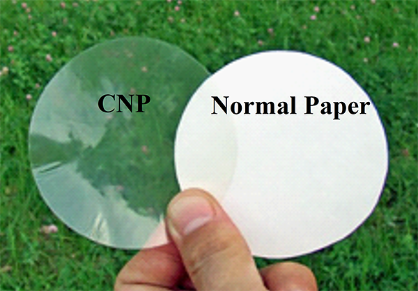 Fig. 3 (a) Transparent CNP. |
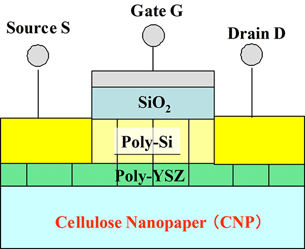 Fig. 3 (b) Final target. |
Key publications
- S. Horita and P. Jain, Dependences of deposition rate and OH content on concentration of added trichloroethylene in low-temperature silicon oxide films deposited using silicone oil and ozone gas, Jpn. J. Appl. Phys., 57, 03DA02 1-7 (2018).
- M. T. K. Lien and S. Horita, Material properties of pulsed-laser crystallized Si thin films grown on yttria-stabilized zirconia crystallization-induction layers by two-step irradiation method, Jpn. J. Appl. Phys., 55, 03CB02 1-8 (2016).
- S. Horita and B. N. Q. Trinh, Disturb-Free Writing Operation for Ferroelectric Gate Field-Effect Transistor Memories with Intermediate Electrodes, IEEE Trans. Electron Devices, 56, 3090-3096 (2009).
Equipment
Nd:YAG laser, Ion implantation, X-ray diffractometer, X-ray photoelectron spectroscopy (XPS), Raman spectroscopy, photolithography
Teaching policy
I would like to foster human resources who can swim across rough sea in development or research race. For the first year, you take course lectures to learn principle and basic knowledge for research. Also, you learn practical knowledge by reading journals and doing basic experiments. In the next year, doing research by yourself, deeply discussing with us, and presenting in conferences, you improve research ability much more.
[Website] URL:https://www.jaist.ac.jp/ms/labs/handoutai/horita-lab/horita.html