Fundamental research on organic semiconductors and their application to optoelectronics
This Lab is not accepting student after October 2026
Laboratory on Organic Optoelectronics
Professor:MURATA Hideyuki
E-mail:
[Research areas]
Optoelectronic devices based on organic semiconductors, Optical wireless communication, Conducting materials
[Keywords]
Organic Light Emitting Diodes, Degradation mechanism of OLED, Fluorescence antenna, Metal fillers made from gold leaf
Skills and background we are looking for in prospective students
We are looking for students who are curious to develop optoelectronic devices based on organic materials. By considering your research experience and scientific background, we will determine your research project.
What you can expect to learn in this laboratory
You will learn fabrication techniques of organic devices using vacuum deposition method or solution process (spin-coating, dip-coating). You will also learn characterization skills of organic devices using several electrical and optical measurements. Besides experimental skills, you may learn fundamental sciences related to organic devices including device physics, materials science and photochemistry. You will also learn essential skills required as a researcher, such as management of research, documentation and presentation skills.
【Job category of graduates】
Researchers and engineers in electronics, chemical, machinery, battery industries, and faculty member in university and national institutes
Research outline
We are working to apply the results of our basic research on organic semiconductors to the development of practical devices such as organic light-emitting diodes (OLEDs) and optical antennas for visible light wireless communication. In collaboration with private sectors, we are developing precise evaluation devices for OLEDs and vacuum sublimation refining devices for organic semiconductor materials. In collaboration with the city of Kanazawa, we are developing filler materials for conductive pastes using Kanazawa gold leaf as a source material. Our goal is to contribute to society through basic research on organic semiconductor devices.
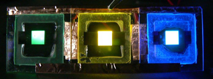 Elucidation of degradation mechanism of OLEDs
Organic EL displays are known for their high image quality, low power consumption, thin and lightweight design, and flexibility, and are already being used in products such as televisions and mobile phones. In the field of organic EL, improving the durability of blue light-emitting materials is an issue that needs to be addressed. The Murata Laboratory is particularly focused on extending the lifespan of devices, and is working to elucidate the degradation mechanisms of blue lightemitting materials while searching for blue light-emitting organic EL materials with high durability. Through our previous research, we have established a system that allows us to consistently carry out research from the fabrication of precise electronic devices to detailed evaluation, and this is also one of our strengths. Recently, we have also succeeded in developing a new evaluation device that can measure displacement current and current-voltage-luminance characteristics continuously and with high precision.
 Development of metal particles for conductive paste made from Kanazawa gold leaf
In this study, we are investigating the application of gold leaf as a conductive filler with the aim of developing new uses for gold leaf. We have found that gold nanoparticles are an excellent material for use as a conductive filler. Recently, we have been working on reducing the cost of conductive fillers.
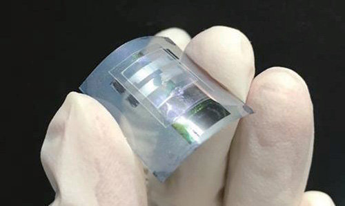
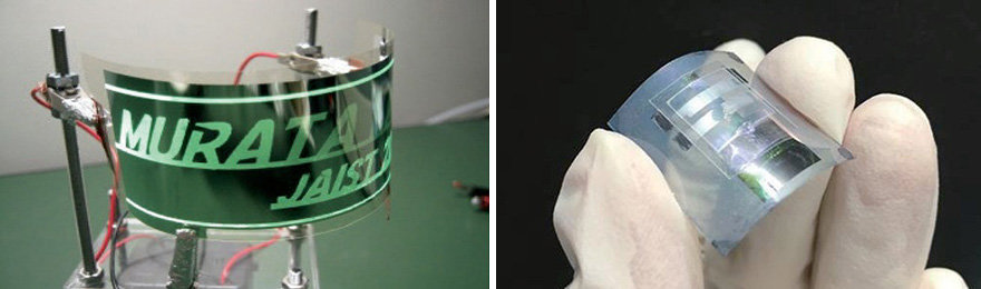 Development of an optical antenna for visible light wireless communication
Visible light wireless communication is attracting attention for its use in short-range communication. We are working on the development of optical antennas for visible light wireless communication that make use of the characteristics of fluorescent dyes. By using Forster energy transfer (FRET) as the light-emitting material for the optical antenna, we have achieved a much higher gain and wider transmission bandwidth than conventional optical antennas, enabling faster data transfer.
Key publications
- C. He, S. Collins, H. Murata, Fluorescent antenna based on Förster resonance energy transfer (FRET) for optical wireless communications, Optics Express, 32, 17152 (2024).
- D. C. Le, D. D. Nguyen, S. Lloyd, T. Suzuki and H. Murata, Degradation of fluorescent organic light emitting diodes caused by quenching of singlet and triplet excitons, J. Mater. Chem. C, 8, 14873 (2020)
- V. Vohra, K. Kawashima, T. Kakara, T. Koganezawa, I. Osaka, K. Takimiya, H. Murata, Efficient inverted polymer solar cells em- ploying favourable molecular orientation, Nature Photonics, 9, 403 (2015).
Equipment
Ultra-high vacuum depositing system,
High vacuum deposition system with glove box
Device characterization system
Photoluminescence quantum yield measurement system, Time-resolved photoluminescence and electroluminescence measurement system
Device stability measurement system
Photoelectron yield spectroscopy, Inverse photoelectron spectroscopy
Teaching policy
During undergraduate education, you may have learnt basic knowledge of your field of expertise. A graduate school is a place to carry out your research using your knowledge with acquiring advanced knowledge. Even if your research goes wrong and you face obstacles, the experience of overcoming difficulties is valuable. I think that a successful experience gives you confidence, and overcoming difficulties bring up you to the next stage.
[Website] URL : https://www.jaist.ac.jp/ms/labs/murata/index.html