Development of nanomaterials based on the understanding of surface and interface
Laboratory on Advanced Nanomaterials Science
Professor:YAMADA-TAKAMURA Yukiko
E-mail:
[Research areas]
Materials Science and Engineering, Surface Science
[Keywords]
nanomaterials, 2D materials, thin films, ultra-high vacuum, hetero-epitaxial growth, surface and interfaces
Skills and background we are looking for in prospective students
We are looking for students who are curious to see how the atoms are aligned at the surfaces and interfaces of materials, and are eager, to understand how these structures determine the properties of materials by carrying out many experiments, calculations, and thinking.
What you can expect to learn in this laboratory
You are expected to use cutting-edge microscopy and spectroscopy systems without destroying them, and to observe crystal and electronic structures which no one has ever seen. Under such circumstances, you have to be cautious and daring at the same time. Quite often, something goes wrong, and things will not proceed as you planned. You will learn to be patient and flexible to accomplish the original goal, and in the end, you will be able to find something totally new and unexpected. Frequent discussions with faculties and fellow students will make you think logically and critically.
【Job category of graduates】
Engineers/researchers in electronics, materials, healthcare, system integrating, machinery industries, and national agencies
Research outline
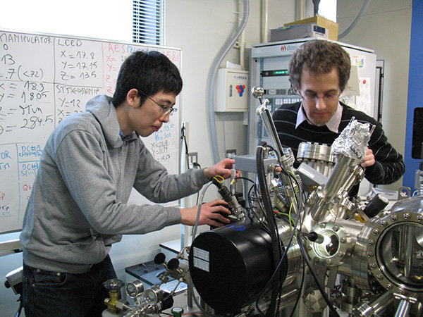 Modern industry is founded on thin film materials technologies, ranging from protective coatings to electronic devices, and in order to improve their performance, controlling film-substrate interfaces would be critical. The surfaces and interfaces become even more important in the growth of nanomaterials and their properties, since the bulk part is reduced and the surfaces and interfaces become dominant. Our group develops new nanomaterials based on the understanding of surfaces and interfaces obtained by using cutting-edge microscopy and spectroscopy systems and by carrying out first-principles calculations.
One of the main research projects in our group is “silicene”, Si-version graphene, and related two-dimensional (2D) materials formed on hetero-epitaxially grown thin films of zirconium diboride (ZrB2). ZrB2 has a very good lattice matching to a wide-gap semiconductor, hexagonal gallium nitride (GaN), and thus, ZrB2 is a promising buffer layer for GaN growth when it is grown on a low cost, large diameter substrate such as Si wafers.
We discovered silicene, in 2012, while trying to understand the surface structure and properties of diboride thin films grown on Si wafers, thanks to close collaboration with a photoelectron spectroscopy group and first-principles calculation group in JAIST. Our findings attracted lots of interests, and collaborations have expanded to other universities and institutions in Japan and overseas. Through such international collaboration, we have recently succeeded in encapsulating silicene under insulating and inert hexagonal boron nitride monolayer which is another interesting 2D material.
We combine many different material characterization techniques, including those carried out at synchrotron radiation facilities, and also perform first-principles calculations to tackle with unique and novel 2D materials. Recently, we have discovered that, on the surface of ZrB2 thin film grown on Ge substrate, 2D Ge layer crystallizes into a structure which we predict to have a “flat band” in its electronic structure.
Even in a material studied by many researchers for a very long time, a big surprise is hidden, which is waiting for you to be discovered. Our students have discovered a new polymorph of a typical layered monochalcogenide, gallium selenide (GaSe), by cross-sectional scanning transmission electron microscopy, and studied its stability and electronic structure by first-principles calculations. You just have to keep your eyes and mind wide open.
We will not limit our research to the above studies. There are numerous surface and interface problems waiting to be solved. We would like to help you find, understand, and solve your own interesting and challenging questions.
Key publications
- First-principles study on the stability and electronic structure of monolayer GaSe with trigonal-antiprismatic structure, H. Nitta, T. Yonezawa, A. Fleurence, Y. Yamada-Takamura, and T. Ozaki, Physical Review B 102, 235407 (2020).
- Emergence of nearly flat bands through a kagome lattice embedded in an epitaxial two-dimensional Ge layer with a bitriangular structure, A. Fleurence, C.-C. Lee, R. Friedlein, Y. Fukaya, S. Yoshimoto, K. Mukai, H. Yamane, N. Kosugi, J. Yoshinobu, T. Ozaki, and Y. Yamada-Takamura, Physical Review B 102, 201102(R) (2020).
- Van der Waals integration of silicene and hexagonal boron nitride, F. B. Wiggers, A. Fleurence, K. Aoyagi, T. Yonezawa, Y. Yamada-Takamura, H. Feng, J. Zhuang, Y. Du, A. Y. Kovalgin and M. P. de Jong, 2D Materials 6, 035001 (2019).
Equipment
Ultra-high vacuum thin film growth system, ultra-high vacuum scanning probe microscopes, thin film X-ray diffraction, synchrotron radiation facilities, supercomputers.
Teaching policy
An originally designed UHV-CVD system with RHEED and a very unique UHVMBE-XPS/UPS-SPM system are installed in MS Building-IV. We welcome those who are interested in carrying out experiments such as film growth and surface/interface analysis with ultimate resolution, and, more important, who are always curious to find out what is really going on.
[Website] URL:https://www.jaist.ac.jp/ms/labs/yukikoyt