Develop Innovative Energy & Environmental Devices using Atom-scale Nanotechnologies!
This Lab is not accepting student after October 2025MIZUTA Laboratory
Professor:MIZUTA Hiroshi
E-mail:
[Research areas]
Graphene sensor/switch, phonon engineering
[Keywords]
NEMS, single molecular sensing, atom-scale fabrication, quantum devices, ab initio simulation
Skills and background we are looking for in prospective students
Understanding of fundamentals is required for at least one of the following: solid state physics, quantum chemistry, semiconductor devices, electrical or mechanical engineering. Students with curiosity, intellectual open-mindedness and interests in working in truly international research group are particularly welcome.
What you can expect to learn in this laboratory
Atomic layer material science such as graphene, h-BN, MoS2 and single-nanometer fabrication technology to develop novel electric-field sensors for lightning forecast, highly functional chemical sensors for skin gas detection, ultra-low-power nano-electro-mechanical (NEM) switches, nanoscale thermal devices and quantum functional devices. Students will learn state-of-the-art technologies such as (1) Electron Beam lithography, Helium ion beam patterning technology and nano-device fabrication processes, (2) Environmentally-controlled 5 - 500 K DC and RF probe stations, dilution refrigerator, Electrical characteristic measurements and (3) multi-scale simulation techniques.
【Job category of graduates】
ICT, manufacturing equipment, precision measurement instruments companies and National research and development agency.
Research outline
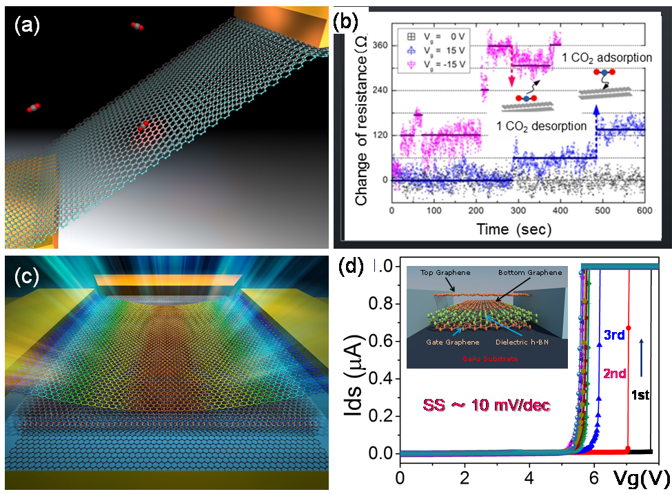
Fig. 1 (a) Schematic of GNEM single molecular sensing, (b) temporal signal of individual CO2 molecule adsorption, (c) schematic of GNEM switch and (d) observed abrupt switching.
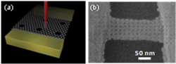
Fig.2 (a) A schematic of nano pore patterning with He+ ion beam and (b) an example of fabricated GPnC.
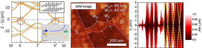
Fig. 3 Energy band structure for bilayer graphene (left), an AFM image of a graphene SCT (middle), and observed Coulomb diamond characteristics (right)
We run an international research group aiming at developing innovative functional devices using graphene and other atomic layer materials. Particularly, we focus on the following research topics:
1) Graphene Nanoelectromechanical (GNEM) sensor and switch devices:
Based on remarkable electronic and mechanical properties of graphene, we develop novel GNEM devices for challenging applications. GNEM sensors enable to detect a single CO2 molecule adsorption [1] as well as zeptogram (10-21 g) order mass change. These sensors are now applied for ppb-level environmental and body gas monitoring. These sensors are now applied to monitor ppb – ppt level human skin gas for early-stage illness detection. We also develop novel electric-field sensors for lightning detection and forecast. GNEM switches feature very abrupt sub-thermal switching (S < 60 mV/dec) at room temperature [2] with low switching voltage. These switches enable remarkable reduction of power consumption of ICs and sensor circuits towards zero power systems.
2) Single-nanometer fabrication technique and nanoscale heat phonon engineering
We develop new atom-scale fabrication technique to curve graphene into single-nanometer (< 10 nm) nanostructures by using focused helium ion beam. Arrays of pores of 3 – 4 nm in diameter (nanomesh) are patterned to fabricate graphene phononic crystals (GPnC) [3] to control heat phonon in the sub – few THz regime. This will enable to control thermal transport at relatively low temperature (< 200°C). Asymmetric nanomesh structures are particularly studied for thermal rectifier applications.
3) Valleytronic devices and Quantum functional devices
We study valleytronics in atomic layer materials such as graphene and MoS2, which have attracted much attention recently for novel ultra-low-power information processing technology. We explore symmetry breaking and the generation of Berry curvature in various structures of stacked atomic layer materials both theoretically and experimentally. We also study carbon based nanomaterials and quantum devices such as single-carrier transistors (SCTs), NV centers in diamond towards quantum information processing and graphene-based tunnel field effect transistors (GTFET). We study the operation mechanism and their performance limits experimentally and multi-scale simulations (first-principles and device level).
Key publications
- J. Sun, M. Muruganathan, and H. Mizuta, ʻRoom temperature detection of individual molecular physisorption using suspended bilayer graphene’, Science Advances 2(4), e1501518 (2016)
- A. Kareekunnan, T. Agari, A. M. M. Hammam, T. Kudo, T. Maruyama, H. Mizuta, and M. Muruganathan, ‘Revisiting the Mechanism of Electric Field Sensing in Graphene Devices’, ACS Omega 6, 34086-34091 (2021).
- F. Liu, M. Muruganathan, Y. Feng, S. Ogawa, Y. Morita, C. Liu, J. Guo, M. Schmidt and H. Mizuta, ‘Revisiting the Mechanism of Electric Field Sensing in Graphene Devices’, Nano Futures 5(4), 045002 (2021)
Teaching policy
We explore a variety of emerging nanotechnologies for 'More-than-Moore' and 'Beyond CMOS' era. We warmly welcome young scientists seeking an active international research environment and innovative atomistic scale devices research.
[Website] URL:https://www.jaist.ac.jp/ms/labs/mizuta-lab/english/index.html