Develop next-generation Si-based solar cells through novel process technologies
Laboratory on Next-Generation Silicon Photovoltaics
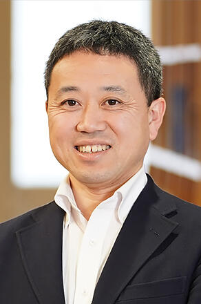
Professor:OHDAIRA Keisuke
E-mail:
[Research areas]
Solar cells, Semiconductor engineering, Thin film formation
[Keywords]
crystallization, passivation, module reliability
Skills and background we are looking for in prospective students
Students are preferred to have basic knowledge of solid-state physics and semiconductors.
Concerns for a global environmental issue and an energy problem may become a driving force to promote their research.
What you can expect to learn in this laboratory
Students can achieve skills for the operation of vacuum equipment, thin-film formation and characterization, device fabrication and characterization by performing their own research. They can also acquire basic academic skills for semiconductors and solar cells through data analysis, daily discussion, and a weekly seminar. Furthermore, students can gain high problem-solving skills, owing to the policy of our group supporting individual initiatives. Presentation and communication skills can be strengthened through presentations in domestic and international conferences and a booth exhibition.
【Job category of graduates】
Post-doctoral researcher in institutes, Manufacture and research work of electronics and materials related companies
Research outline
Solar cells based on silicon, which is highly abundant on the earth, dominate the present market share of photovoltaic technologies, and is expected to be the leading player also in the future. At the same time, the development of solar cells with lower cost, higher efficiency, and long-term reliability are necessary, and further technological breakthroughs are required. Our group focuses on the following research topics and attempts to establish the basic technology of silicon-based high-performance solar cells.
1.Formation of polycrystalline silicon films for solar cells by rapid annealing
Flash lamp annealing (FLA), millisecond-order discharge from Xe lamps, can supply pulse light with a fluence of several tens of J/cm2, which momentarily corresponds to several tens of thousands times as much as sun-light on the earth. Our group investigates the formation of polycrystalline silicon (poly-Si) films on low-cost glass substrates for cost-effective solar cells. Poly-Si films with a thickness of >4 µm can be formed by supplying a single shot of flash lamp pulse on precursor amorphous silicon (a-Si) prepared on glass substrates. When hydrogenated a-Si films are used as precursor films, hydrogen atoms remain inside the silicon films even after crystallization, which can contribute to the termination of dangling bonds in the poly-Si and the formation of poly-Si films with low defect density. Our group investigates the fundamental mechanism of the crystallization of a-Si films by FLA and the application of the poly-Si films to thin-film crystalline silicon solar cells.
2.Application of catalytic chemical vapor deposition (Cat-CVD) to the fabrication of solar cells
Cat-CVD, a film deposition method through the catalytic cracking of gas molecules on a heated catalyzing wire, can reduce damage to a sample surface due to its plasma-damage-less nature, and can produce high-quality passivation films which can significantly suppress the recombination of minority carriers on the surface of crystalline silicon and lead to the realization of high-efficiency crystalline silicon solar cells. Cat-CVD apparatus can also be utilized for the doping of B or P atoms to the surface of silicon samples by exposing to B- or P-related radicals formed by the catalytic cracking of B2H6 or PH3. This novel process, catalytic impurity doping (Cat-doping), can be applied to the formation of front- or back-surface field layers and doping layers in crystalline silicon solar cells.
3.Reliability and novel structure development of crystalline silicon photovoltaic modules
The performance degradation of photovoltaic modules owing to a voltage between a module frame and cells, potential-induced degradation (PID), is a crucial issue particularly in large-scale photovoltaic power plants in which a number of cells and modules are connected in series. We investigate the mechanism of the PID of crystalline silicon photovoltaic modules and develop measures for the suppression of the PID. In addition, components in the present conventional modules are adhered with encapsulant. This causes various types of degradation originating from the encapsulant and makes it difficult to sort and recycle the components when disposing of the modules. To solve this problem, we are also developing new-type photovoltaic modules with no encapsulant.
Key publications
- K. Ohdaira, M. Akitomi, Y. Chiba, and A. Masuda, Potential-induced degradation of n-type front-emitter crystalline silicon photovoltaic modules — comparison between indoor and outdoor test results, Sol. Energy Mater. Sol. Cells 249, 112038 (2023).
- R. Ohashi, K. Kutsukake, H. T. C. Tu, K. Higashimine, and K. Ohdaira, High passivation performance of Cat-CVD i‑a-Si:H derived from bayesian optimization with practical constraints, ACS Appl. Mater. Interf. 16, 9428(2024).
- Z. Wang, H. T. C. Tu, and K. Ohdaira, Formation of n-type polycrystalline silicon with controlled doping concentration by flash lamp annealing of catalytic CVD amorphous silicon films, Jpn. J. Appl. Phys. 63, 105501 (2024).
Equipment
FLA system
Cat-CVD chamber
Solar cell characterization system
Photovoltaic module fabrication and characterization system
Thin-film characterization system
Teaching policy
Our group has a policy of supporting students’ individual initiatives, and their own ideas can be included in their researches. A morning meeting is held every weekday, and the activities of each student are shared. Students can also have simple research discussion in the meeting. In a study meeting, held on every Saturday, a duty student is required to explain the detail of a journal paper and to answer questions from other students and staffs, by which students can obtain high basic academic skills. Students can actively present their research achievements, and acquire ability to write their own research paper for themselves.
[Website] URL : https://www.jaist.ac.jp/ms/labs/ohdaira/en/home_e