
| Text Size: A A A A |
|
JAIST-CNSI Workshop 2010 |
 |
Masaru Kawakami, JAIST Lecturer, School of Materials Science | |||
| Dynamic Force Spectroscopy reveals the fluctuation of protein molecules | ||||
|
In physiological conditions, biomolecules are designed so that their conformation fluctuates dynamically in order to execute their biological functions. Therefore an understanding of the fluctuation is necessary for a full understanding of the function of the protein molecules.
Atomic Force Microscopy has evolved into a powerful technique for investigating the dynamics of protein molecules at single molecule level. Mechanical tension is applied to individual molecules, and the subsequent, unfolding event is recorded in force extension traces. Using Bell’s theoretical model and Monte Carlo simulation, the unfolding force data at various pulling velocity can be analyzed and we obtain the energy landscape profile of the molecule, i.e. the distance between the native state and transition state (xu) and unfolding rate constant at no force (ku). ku is related to the activation energy of the mechanical unfolding (∆G*0 by the Arrhenius equation ∆G*0 = kBT ln(A/ku), where A is the Arrhenius pre-factor).
Recently we have proposed that the protein spring constant D can be estimated assuming a parabolic function for the free energy, G(x) = 1/2•Dx2, analogically to the potential energy of Hooke’s spring and the amplitude of fluctuation x along the pulling direction can be estimated by the equipartition theorem.
In the presentation, we will show the recent results using this approach with two proteins (titin and protein L), and discuss how temperature and mutations affect the internal fluctuation of protein molecules.
References
|
 |
Yuichi Hiratsuka, JAIST Lecturer, School of Materials Science | |||||
| Micro-mechanical devices powered by motor proteins | ||||||
|
Living system use many types of micro or nano-mechanical systems, which are called "motor protein". Those biological motors have unique features, such as nano-meter scaled molecular motor, high efficiently energy transduction from chemical energy or having a capacity of self-assembly. The realization of bio-hybrid micro-machines to integrate such motor proteins and micro- or nano-structures fabricated of inorganic materials, would have some potential values that are not achieved by traditional electronic, magnetic or optical devices. In this workshop, I will introduce our two mechanical devices driven by biological motors: 1) micro-rotary motor driven by kinesin-microtubule motor system, 2) optical device driven by motor protein (mimic fish melanophore cell system). We believe that such studies contribute to the development of micro-devices assembled from the bottom-up.
References
|

 |
Hieu Chi Dam, JAIST Lecturer, School of Knowledge Science | |||||||
| Pt nanoclusters on carbon nanotube supports | ||||||||
|
The catalysis plays an innovative role in developing new technologies and catalyst design has become a big issue in industrialization. The combination of nanoclusters and the carbon nanotube supports are strongly proposed as a solution for superior heterogeneous catalysis. Recently we succeeded in establishing a new concept, based on a fundamental bottom-up approach, for synthesizing highly dispersed and size-controlled nanoparticles on carbon nanotube supports. From a theoretical viewpoint, it is suggested that the mixing of the wave functions of the nanotubes and those of the atoms and nanoclusters determine the geometric, electronic, and therefore catalytic properties of the adsorbed clusters.
In this paper, we report our studies on the interplay between single-wall carbon nanotube (SWNT) supports and adsorbed Pt clusters atoms using the first-principles density functional theory (DFT). The cluster formation process, stabilities, electronic structures, and gas adsorption properties of Pt clusters on SWNT will be discussed from the viewpoint of catalyst design.
References
|

 |
Taku Hasobe, JAIST Lecturer, School of Materials Science | |||||||||||||||||||||
| Construction of Supramolecular Assemblies for Photovoltaic Application | ||||||||||||||||||||||
|
Increased efforts to assemble dye molecules into desired structures have been made because of their extended p-electron conjugation. Recent developments in synthetic and supramolecular techniques have made it possible to precisely control and organize molecules at the nanometer level. Such strategies enable us to construct molecular assemblies possessing photovoltaic functionalities. In photovoltaic cells, the following three processes such as light- harvest, charge separation, and carrier transport are generally required. Therefore, construction of supramolecular assemblies possessing these three processes are interesting and promising for future development of photovoltaics.1
In this presentation, the focus is
our recent supramolecular possessing functionalities, which are mainly composed of porphyrin dyes and nanocarbon materials such as fullerenes and carbon nanotubes.2-10 The details of preparation method, structural and photoelectrochemical properties will be discussed.
References
|

 |
Rainer Friedlein, JAIST Lecturer, School of Materials Science | |||||
| Bonding and electronic states at organic/metal interfaces with strong interactions | ||||||
|
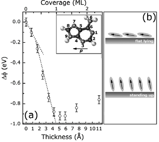
The control of the structural ordering and electronic properties at organic/metal hybrid interfaces represents a necessary prerequisite for achieving highly-efficient organic electronic devices. In this context, the results of angle-resolved, ultraviolet photoelectron spectroscopy (ARUPS) measurements of the electronic structure of two long-range, highly-ordered thin film systems, at sub-monolayer or monolayer coverage, are reported: anthracene and adenine on Cu(110). The particular molecular systems have been chosen to provide answers on different questions: For anthracene, a comparison with the larger pentacene molecule is useful to understand the dependence of interfacial states on the interaction strength at the interface. In the case of adenine, it is interesting to find out how interfacial states evolve as a function of the molecular orientation.
Both molecules interact strongly with the Cu(110) surface resulting in the formation of interface states formed by hybridization with Cu (3d) orbitals, and by a substantial re-distribution of interfacial electronic densities. For the anthracene monolayer on Cu(110), spectral features observed in the binding energy region of 2-4 eV are assigned to hybrid interfacial states similar to those observed for pentacene on the same surface [2]. A peak in the vicinity of the Fermi level is formed upon (partial) charge transfer from 4s states into the LUMO but involves some degree of hybridization with Cu (3d) orbitals. Differences to the pentacene monolayer relate in particular to the strength of hybridization that depends strongly on the energetic separation between the Cu (3d) band and the molecular levels.
The room temperature growth of adenine on Cu(110) is characterized by the occurrence of a coverage-dependent reorientation mechanism where molecules change from "flat-lying" (low coverage) to a "standing-up" (high coverage) configuration [3]. During this transition, hybrid interfacial states do not change significantly demonstrating the validity of a common mechanism for the formation of these states. The discussing focuses also on the influence of the intrinsic dipole molecular moment in determining the vacuum level alignment as a function of the film thickness.
References
|
 |
Yukiko Yamada-Takamura, JAIST Lecturer, School of Materials Science | |||||
| Epitaxial diboride thin films for integration with III-nitrides | ||||||
|
Materials in the form of thin films save valuable resources, and moreover, allow us to integrate different materials easily. New phases and structures realized through the integration as well as the improvement of properties in the integrated systems bring us surprises, and interfaces formed between very different materials have many possibilities yet to be explored.
Our research interests focus on the epitaxial growth of refractory and metallic diboride thin films and their integration with other materials, especially III-nitrides (1-3). Metallic diborides with a simple crystal structure consisting of alternating hexagonal close-packed metal layers and honeycomb boron layers are themselves interesting materials, but could be even more so through such integration. For example, zirconium diboride (ZrB2), which has a very good lattice matching (0.6 % mismatch) to a wide-gap semiconductor, gallium nitride (GaN), has a lot to offer in the form of epitaxial thin film: buffer layer, light reflector, heat-resistant electrode, etc. ZrB2 film could be a good growth template layer for GaN growth on low cost, large diameter substrates, such as silicon wafer. And at the same time, it could be a heat-resistant electrode, which is necessary for high power devices. Furthermore, superlattice of semiconducting GaN and metallic ZrB2 would be an interesting material to explore, if alternating epitaxial growth of two materials were realized.
In order to grow diboride films with high purity and high crystallinity, the understanding of growth process and the control of surfaces and interfaces would be critical. We chose chemical vapor epitaxy (CVE) from zirconium borohydride ( Zr(BH4)4 ) for the growth of ZrB2, because of its advantage in highly pure source material compared to sintered solid targets used in sputtering and pulsed laser deposition processes. A unique ultrahigh vacuum - CVE system, which has a capability of monitoring the film growth in-situ using reflection high-energy electron diffraction, was constructed. Hetero-epitaxial growth of ZrB2 thin films and the result of their characterizations will be reported, and their possible integration with nitrides will be discussed.
References
|
 |
J.D. Lee, JAIST Lecturer, School of Materials Science | |||||||||||||||||
| Universal fluorescence intermittency of nanoscopic light emitter : New model and new challenge | ||||||||||||||||||
|
In spite of the importance for both fundamental scientific profundity and technological applications, the origin of quantum dot fluorescence intermittency has remained an open problem under high controversy since the first experimental observation in the spectrum of Ba+ ions in a radio-frequency trap [1, 2]. Based on the many-body time-dependent approach [3, 4], we propose a new microscopic quantum mechanical model incorporating the random tunneling fluctuation between quantum dot and trapping state in order to describe the nonstochastic dynamics of the light-emissive quantum dot [5, 6]. Even if the microscopic nature of the random tunneling fluctuation depends on a specific system, we find that the fluorescence intermittency shows the universal power-law behavior with an exponential bending tail, being insensitive to the specific details. The power-law exponent θ and the crossover time τc characterizing the intermittency statistics through the on-time (τ) probability P(τ) ∝τ-θ(τ ≲ τc ) and ∝e-гτ (τ ≳ τc ) are investigated under the external optical field with its energy ω and intensity A in both numerical and analytic fashions. Dependences of τc and θ on the field intensity A or tunneling intensity v0 are investigated in given limiting situations. Especially, the field-intensity- dependence of τc can be discussed by directly comparing with the recent experiment by Peterson and Nesbitt [7]. The model can be extended beyond a
single quantum dot to consider the Coulomb repulsion between neighboring quantum dots fallen in the ionic states. The interaction gives rise to the memory loss of the dynamics, i.e., the deviation from the power-law (long-memory dynamics) as shown in Fig.1. Besides, the intensified blinking intermittency and enhanced fluorescence are observed as effects of the interaction, consistent with the recent experiment of the assembled CdSe-ZnS quantum dots [8].
References
|

 |
Ryo Maezono, JAIST Lecturer, School of Information Science | |||||
| Bulk modulus enhancement of silicon nanocrystals | ||||||
|
With development of synthesis technique, nano-clusters are intensively studied attracting interests in those novel properties. Since their structures are difficult to be controlled and identified experimentally, first-principles electronic structure calculations are expected to be a useful tool to understand/predict what occurs in experiments. The clusters are regarded as appropriate systems to realize the crossover between bulk and surface electronic structure, it is interesting in theoretical view point as well. As its mechanical property, the possibility of bulk modulus enhancement is reported experimentally in several clusters than those of bulk crystals [1,2]. It is, however, difficult to investigate further by experiments because of the size distribution of clusters scattering around, and hence we studied it by using ab-initio DFT and QMC calculations, applying them to Si_87H_76 system specifically. In LDA it is predicted the modulus at V=10 nm3, corresponding experiments, being slightly enhanced than the bulk crystal values. The prediction, however, critically depends on which kind of exchange-correlation (XC) potentials are adopted in DFT. Indeed it is generally known that GGA, instead of LDA, gives softer modulus. Recently Quantum Monte Carlo (QMC) techniques are applied to ab-initio treatments in materials science [3], which give more reliable predictions about the interacting electronic systems, not relying on XC potentials. We evaluated the bulk modulus by these methods [VMC (variational QMC) and DMC (diffusion QMC)] as well, and found that the DMC results, as a more reliable prediction, supports LDA rather than GGA in this system.
* This work is done in collaborating with Dr. Priya Mahadevan group (Kolkata, India) and Dr. Nguyen Thanh Cuong. References
|
