Create new high-performance electron devices using functional materials
*This Lab. is not accepting new student.TOKUMITSU Laboratory
Professor:TOKUMITSU Eisuke
E-mail:
[Research areas]
Semiconductor devices, Electronic materials
[Keywords]
thin film transistor, oxide semiconductor, ferroelectric material, nonvolatile memory
Skills and background we are looking for in prospective students
Basic knowledge of physics and chemistry, and electrical engineering. Intellectual curiosity and challenging spirit to try to make something new. Logical thinking ability to analyze experimental results.
What you can expect to learn in this laboratory
The objective of the laboratory is to create novel electron devices by utilizing functional materials such as oxide semiconductors and ferroelectric materials. In addition, new concepts and structures of electron devices have been investigated. The members of this laboratory learn basic knowledge of device physics, thin film deposition and device fabrication process along with evaluation technologies of thin films and electron devices.
【Job category of graduates】
Manufacture, development and research work of electronics- and materials-related companies
Research outline
We create new electron devices using functional materials. Recent research activities include large-charge-controlled thin film transistors, solution process of oxide thin films (ferroelectric films and semiconductors), and device fabrication using chemical solution deposition.
1. Large-charge-controlled thin film transistor
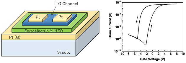
Fig.1 Schematic illustration of ITO channel ferroelectric (Y-HZO)
gate thin film transistor prepared by solution process and
obtained transfer characteristics.
Since ferroelectric materials have non-volatile memory function in its nature, they are used for non-volatile memory integrated circuits. In addition, ferroelectric materials have one more interesting feature, that is a fact they can induce very large charge density compared to conventional dielectric materials. For instance, maximum induced charge density of SiO2 which is common insulator of silicon MOSFET, is limited to 3.5 μC/cm2 at a breakdown electric field of 10 MV/cm, whereas the ferroelectric materials such as PZT can induce as large as 50 μC/cm2 at even 0.5 MV/cm. We have proposed a new concept of thin film transistor (TFT) with conductive channel controlled by the anomalously large charge density of the ferroelectric gate insulator. Until now, we have developed indium-tin-oxide (ITO) channel TFTs, transparent nonvolatile memory TFTs, and flexible oxide channel TFTs using this concept.
Recently, HfO2-based oxide has attracted attention as a new ferroelectric material. In our laboratory, we have used Y-doped Hf-Zr-O (Y-HZO) as a gate insulating film and ITO as a channel layer to fabricate a ferroelectric gate thin film transistor as shown in the figure, and excellent electrical properties have been obtained. Both Y-HZO gate insulator and ITO channel layer were fabricated by the chemical solution process.
2. Control of ferroelectric phase in HfO2-based thin films
HfO2-based oxides, whose ferroelectricity was found recently, are one of the key materials for future electronics, promising for non-volatile memories and transistors that realize steep switching. HfO2 has several crystalline phases; monoclinic, orthorhombic, and tetragonal, and it is necessary to form the meta-stable orthorhombic phase to exhibit ferroelectricity. Usually, elements such as Si and Y are doped to stabilize the ferroelectric phase, but it was pointed out that the introduction of oxygen vacancy stabilizes the ferroelectric phase. In our laboratory, it was found that when the HZO films, formed by the solution process and the sputtering, were crystallized under a reduced pressure, the orthorhombic phase was obtained, showing good ferroelectricity and improvement of the stability of the ferroelectric phase. We are investigating new artificial control methods of the oxidation state in the HfO2-based thin films, using an oxygen scavenging layers, and irradiating atomic hydrogen to intentionally introduce oxygen vacancies, etc. We aim to stabilize the ferroelectric orthorhombic phase and obtain excellent ferroelectricity.
Key publications
- Yuki Hara, Mohit, Tatsuya Murakami, Shinji Migita, Hiroyuki Ota, Yukinori Morita and Eisuke Tokumitsu, “Impact of reduced pressure crystallization on ferroelectric properties in hafnium-zirconium dioxide films deposited by sputtering”, J. Appl. Phys. 60, SFFB05 (2021).
- Mohit, Shinji Migita, Hiroyuki Ota, Yukinori Morita, and Eisuke Tokumitsu, “Thermal stability of ferroelectricity in hafnium–zirconium dioxide films deposited by sputtering and chemical solution deposition for oxide-channel ferroelectric gate transistor applications”, Applied Physics Express, 14, 041006 (2021) .
- Mohit, Takaaki Miyasako, and Eisuke Tokumitsu, “Indium oxide and indium-tin-oxide channel ferroelectric gate thin film transistors with yttrium doped hafnium-zirconium dioxide gate insulator prepared by chemical solution process”, Jpn. J. Appl. Phys., 60, SBBM02 (2021).
Equipment
Rapid thermal annealing (RTA)
Sputtering system
Ferroelectric material evaluation system
Teaching policy
In our laboratory, in order to create a new electronic device, we have to know the features of functional materials and use them properly for devices applications. To realize this purpose, we should have basic knowledge of physics and chemistry to understand material physical properties, along with operation principles of devices. We also need flexible thinking, innovative ideas, crucial decisions. Let’s consider these factors together through experiments and propose a new device of your own idea by the end of the course.
[Website] URL:https://www.jaist.ac.jp/ms/labs/tokumitsu/