
- HOME
- Nanoscale thermal engineering with graphene nanomesh devices
Nanoscale thermal engineering with graphene nanomesh devices
Graphene nanomesh device
In the Mizuta lab, the thermal rectification phenomenon has been observed with a high ratio up to 60% on suspended asymmetric graphene nanomesh devices at low temperatures (150K and 250K). we introduce graphene nanomesh as an artificial phononic crystal structure on half the area of the heat flux channel by Helium Ion Beam Milling technology (HIBM) or Gas Field Ionization Ion Source (GFIS). The nanopore diameter is 6 nm approximately, and the pitch is 20 nm. The heat flux was successfully measured by the 'differential thermal leakage' method. As far as the mechanism of thermal rectification in nanoscale is still not clear, the research is focused on experiments (Nanodevice fabrication) as well as theoretical studies (DFT, Molecular Dynamic and finite element analysis).
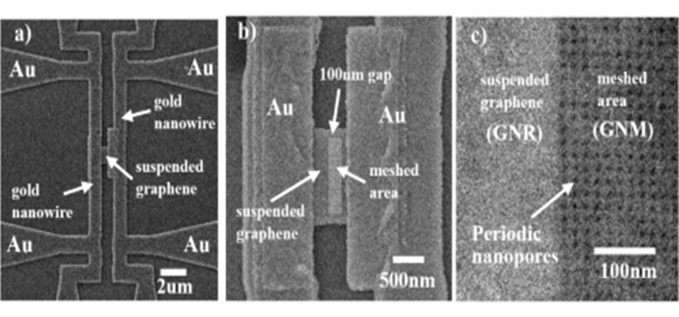
Graphene nanomesh device
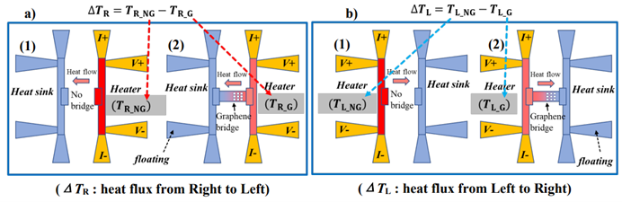
"Differential thermal leakage" measurement method
Analysis of phononic band gap using two-dimensional finite element analysis
Research on the thermal phonon control of graphene is very few and an efficient structure has not been elucidated. Also, actually, it is not easy to process to the target hole size and spacing in the fabrication of graphene devices with periodic nanopore structures because the nanopores are so small. Therefore, in this study, we are considering for the structure that the phononic band gap (PhBG) appears in the THz region using finite element analysis.
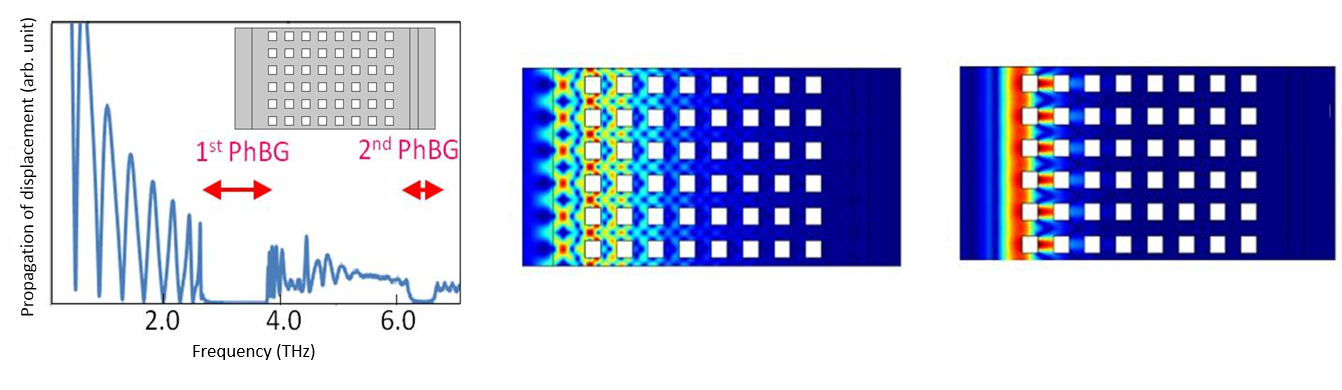
A phonon propagation spectrum in nanopore structure (left), two-dimensional phonon distribution near the 1st PhBG (center) and near the 2nd PhBG (right)
Fabrication of device with periodic nanopore structure
Realizationof the nanoscale periodic pore structure required for graphene phononic device is not easy with the accuracy of conventional fine processing techniques. In this laboratory, we fabricate the device using fine processing equipment with gas field ion source (GFIS) and helium ion microscope (HIM).
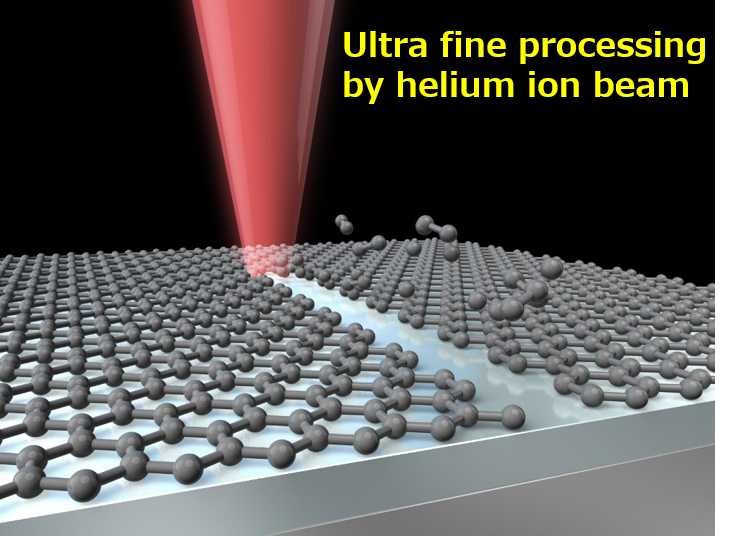
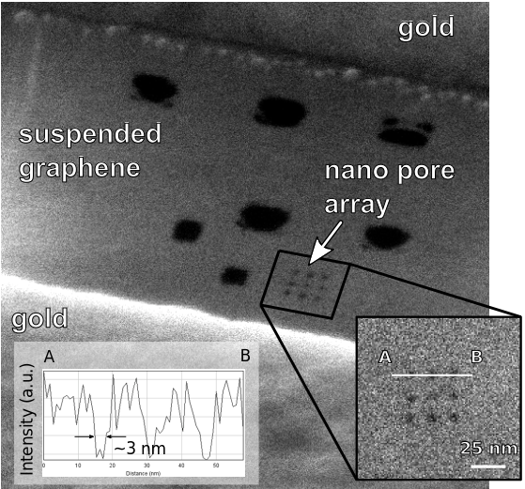
Image of fine processing by HIM Periodic nanopore structure fabricated by HIM
 School of Materials Science, Japan Advanced Institute of Science and Technology