
- HOME
- OUTLINE
OUTLINE
We fabricate micro- and nano- scale graphene and other 2D van der Waals (vdW) hereto-structures devices to study flavor sensors, lightning sensors, thermal diodes and valleytronics.
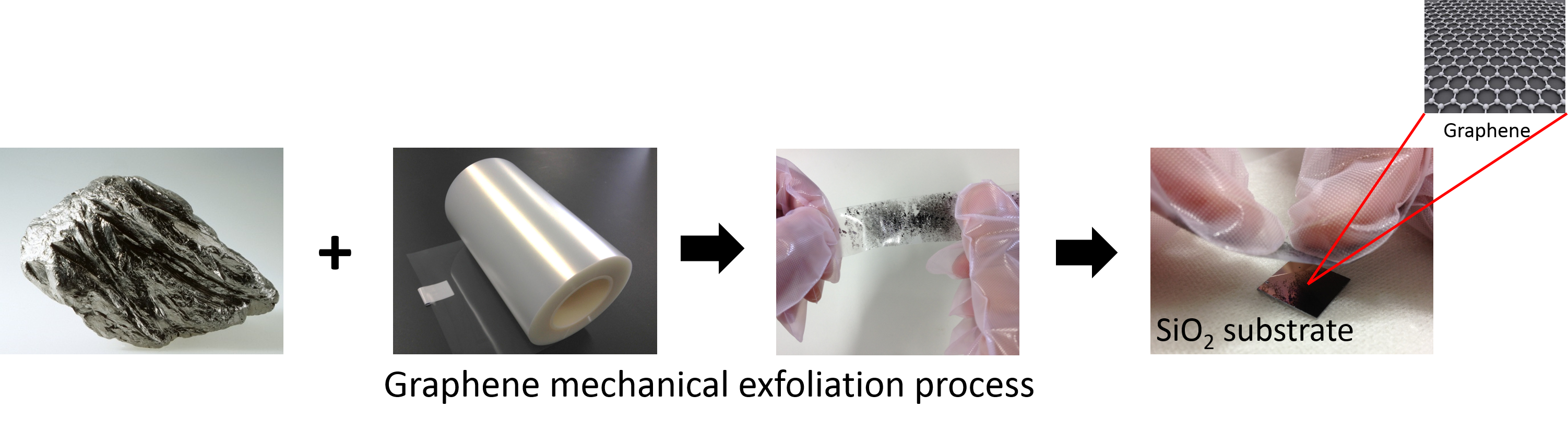
Graphene
Graphene is a two-dimensional material with one carbon atom thickness in a hexagonal lattice structure. Since it has extremely high carrier mobility and excellent mechanical stability, it can be used as a post-silicon material for high performance electronic devices, highly sensitive sensors, NEMS, quantum information processing devices, and a wide range of other applications.
Graphene NEMS (Nano Electro Mechanical System) functional device
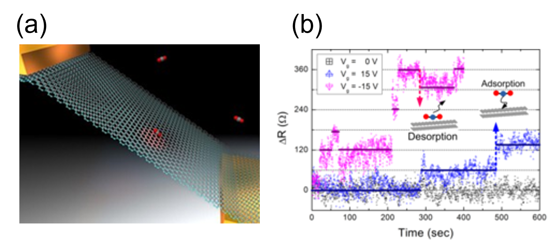
(a) Graphene NEMS functional device
(b) Detection of the individual CO2 molecule
adsorption and desorption in the GNEM device
There is an increasing demand for body gas monitoring technology that enables the early detection of diseases by detecting trace gases emitted from the various parts of human body. As compared to other diagnostic techniques, skin gas analysis is non-invasive and suitable for continuous monitoring. But, these sensors require the parts-per-billion (ppb)-level detection limit. Towards this direction, we are developing sensing devices to realize ultra-high sensitivity gas sensors. Conventional semiconductor technology is not able to reach this ultra-high sensitivity limit.
Graphene is a promising candidate for gas sensing due to its excellent electronic characteristics such as high mobility, low noise, etc. Moreover, monolayer graphene has the largest surface area to volume ratio, which is important for sensing applications. To realize ultra-high sensitivity sensors, we are working on the functionalized graphene sensor based on three sensing methodologies of charge, mass, and molecular vibration sensing in the graphene. We have already reported the single CO2 molecules sensing in the suspended Graphene Nano-Electro-Mechanical (GNEM) devices.
![]()
Electric Field Sensing in Graphene Device
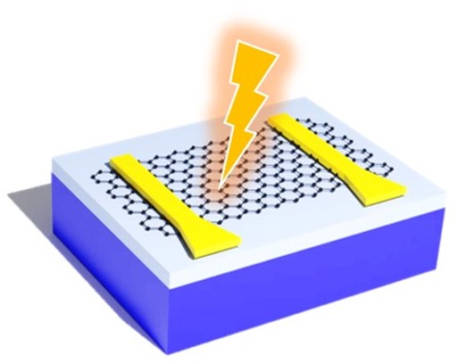
Electric Field Sensing in Graphene Device
Lightning causes human lives and massive economic loss. Thus the early prediction of lightning is vital for preparing ourselves for the disaster. Current lightning detectors detect the electromagnetic waves emitted by lightning flashes. However, detecting the electric field formed between the cloud and ground due to the accumulation of charges has the potential to predict dangerous thunderclouds that accumulate electricity before it strikes. We are currently working on the development of an ultra-sensitive electric field sensor based on graphene. The peculiar energy dispersion of graphene makes it highly responsive to the electric field. This research is conducted in collaboration with OTOWA ELECTRIC CO., LTD.
![]()
Nanoscale thermal engineering with graphene nanomesh devices
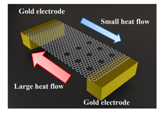
Thermal rectifier based on asymmetric
graphene nanomesh
We aim to precisely control heat (phonon) by using asymmetric graphene nanomesh structures. The advanced helium ion beam milling technology is used to pattern the sub-10 nm periodic nanopores on a suspended graphene ribbon, and form the graphene nanomesh. Currently, we are working on the development of a high-performance thermal rectifier, which can only allow the heat to transfer from one direction. This study will hopefully contribute to the integrated circuit heating problem, as well as the newly emerged thermal storage and thermal information logical processing technologies.
![]()
Two-dimensional material valleytronics research
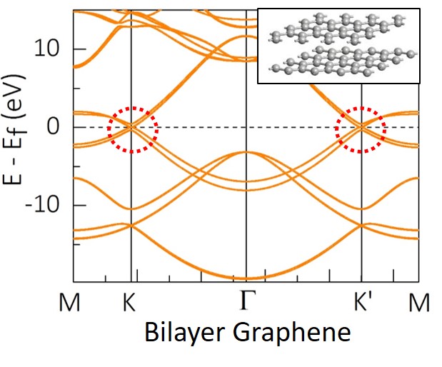
Band structure of bilayer graphene showing
the valley-shaped bands around
the Fermi level at K and K' points
Valletronics, which utilizes the valley degree of freedom of atomic layer materials as a new information carrier, is expected to be a future information processing technology that goes beyond conventional electronics and spintronics.
We are researching valleytronics in atomic layer materials such as graphene and MoS2, which have attracted much attention recently. We explore symmetry breaking and the generation of Berry curvature in various structures of stacked atomic layer materials both theoretically and experimentally.
![]()
Ab-initio simulation
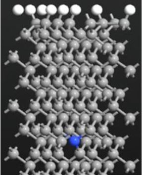
Crystal structure of nitrogen vacancy(NV)
center diamond with hydrogen-terminated
surface
The fundamental basis for the study of condensed matter physics and the study of materials is to understand the behavior of electrons in an atom or a molecule under varied conditions. The electrical, optical, and magnetic properties of a material rely on how the electron acts itself in the material. First-principles calculation method attempts to solve the fundamental equation of quantum mechanics to obtain information on such properties of electrons in a material. Here we use various software to create desired atomic and molecular structures and to perform the first-principles calculation of various quantum structures based on monolayer materials and diamond by using the state-of-the-art super-computing facility available at the institute. We also conduct a large-scale simulation by combining the first-principles calculation and nonequilibrium quantum transport theory.
![]()
 School of Materials Science, Japan Advanced Institute of Science and Technology