Equipment
If you would like processing, measurement, etc., please do not hesitate to contact us.
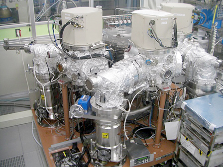
Thin-film deposition and processing equipment
Flash lamp annealing (FLA)Techno Research Ltd. (Xe lamp: ORC Manufacturing Co., Ltd.)
Millisecond-order annealing can be performed by using a pulse light from a Xe lamp.
A pulse light with a fluence of >10 J/cm2 and a duration of 1-10 ms can be obtained.
This is utilized e.g. for the crystallization of Si films.
The irradiation area is 2×2 cm2.
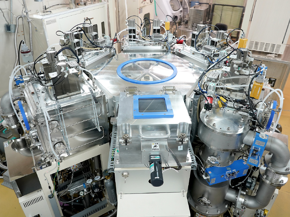
Cat-CVD for photovoltaicsDesign System Co., Ltd.
There are totally 6 chambers (for load lock, n-type a-Si, p-type a-Si, intrinsic a-Si, SiNx, and general purpose) in this Cat-CVD system.
Substrates with a size of up to 156×156 mm2 can be installed.
This system is used for the deposition of passivation films for crystalline Si and for the fabrication of Si heterojunction solar cells.
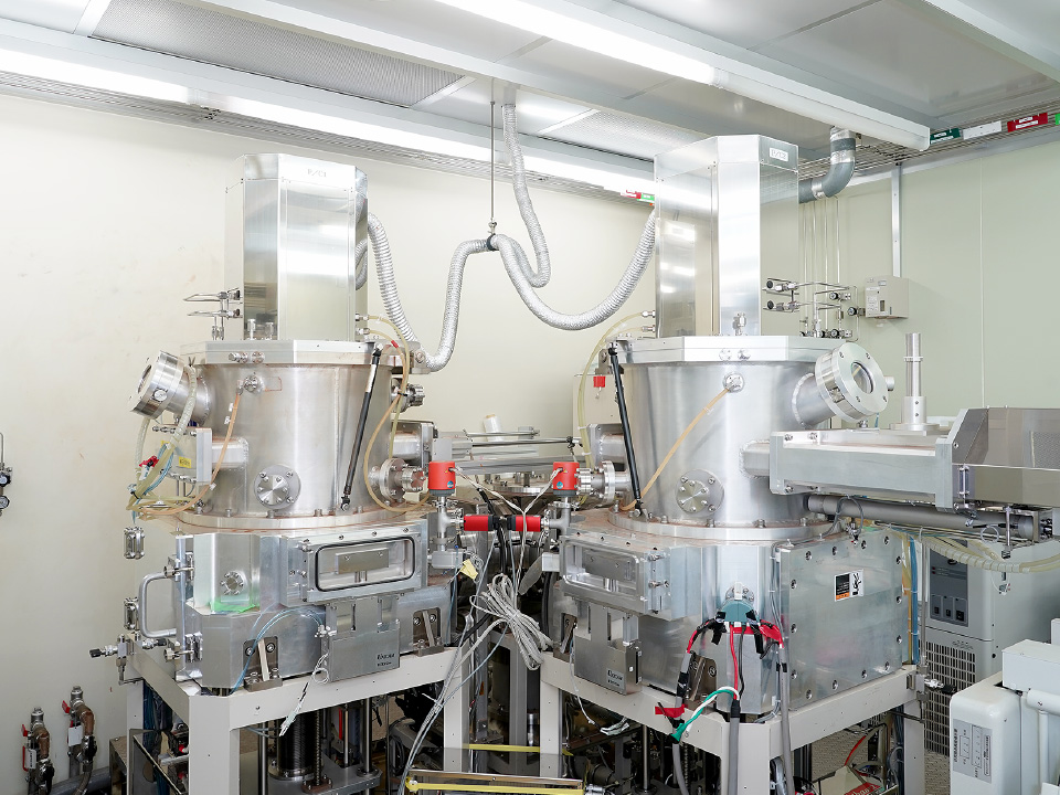
Cat-CVD for Si film depositionIshikawa Seisakusho, Ltd.
8-inch wafers can be installed into this large-sized Cat-CVD.
There are two chambers for the deposition of SiNx and a-Si films.
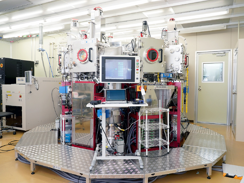
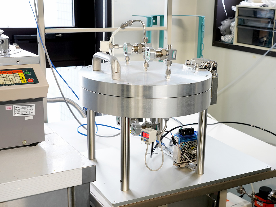
Vertical-type Cat-CVDVIC International Co., Ltd.
Substrates are set vertically in this Cat-CVD, similar to the mass-production Cat-CVD system.
Substrates with a size of up to 156×156 mm2 can be installed.
Cat-CVD for the deposition of passivation films Canon ANELVA Corporation
This face-down Cat-CVD system, with 3 chambers for intrinsic a-Si, doped a-Si, and SiNx, is mainly used for the deposition of passivation films for crystalline Si.
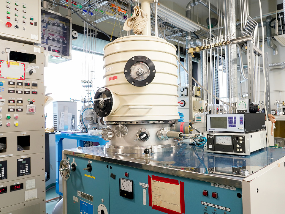
Vacuum evaporationShowa Shinku Co., Ltd., SNC-06D
The vacuum evaporation can form thin films by vaporizing materials on a conductively-heated boat.
This is used for the formation of metal films such as aluminum.
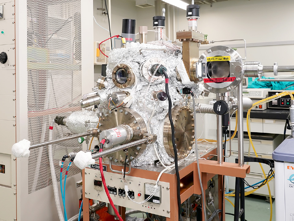
Electron-beam (EB) evaporationCanon ANELVA Corporation, L-300E-TL
The EB evaporation system can form thin films by vaporizing materials in a crucible by irradiating an electron beam.
This is used for the formation of thin films such as Si with high melting point.
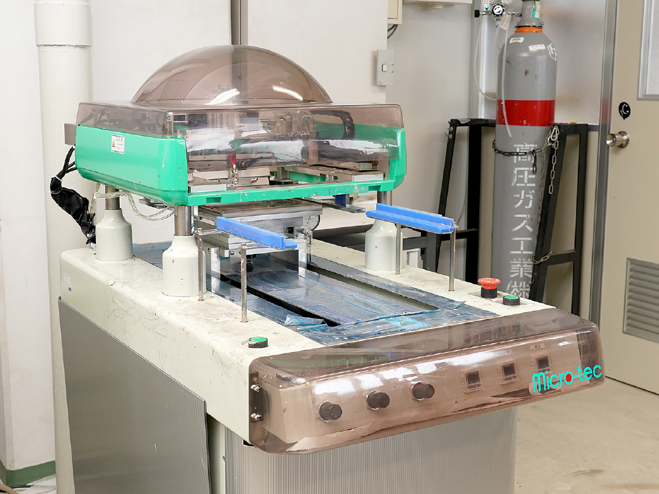
Screen printerMicro-tec Co., Ltd, MT-320
Patterns are printed by pushing paste with a squeegee through a screen mask. This is used for the printing of electrodes for solar cells.
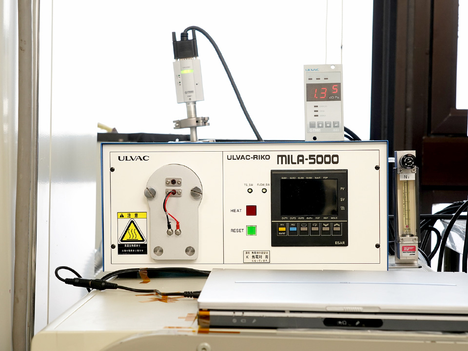
Rapid Thermal Annealing (RTA)ULVAC TECHNO, Ltd., MILA-5000
This RTA system is for 2×2 cm2-sized samples, and is used for the fabrication of solar cells.
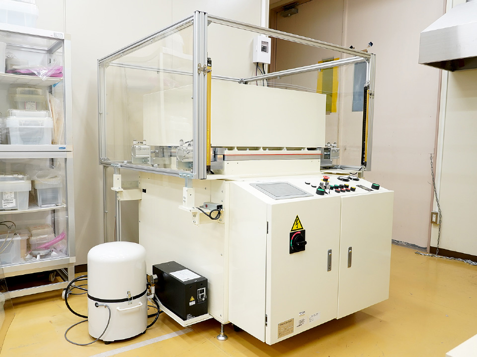
Module laminatorNPC incorporated, LM-50X50-S
This is a laminator in which industrial-sized photovoltaic modules can be fabricated.
Module laminatorDesign System Co., Ltd.
This laminator is to fabricate small-sized photovoltaic modules. The modules with a size of up to 18×18 cm2 can be fabricated in this system.
Evaluation equipment
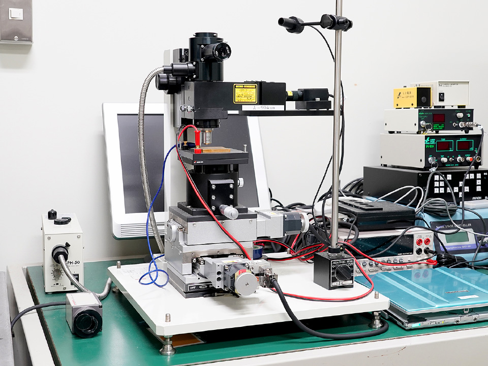
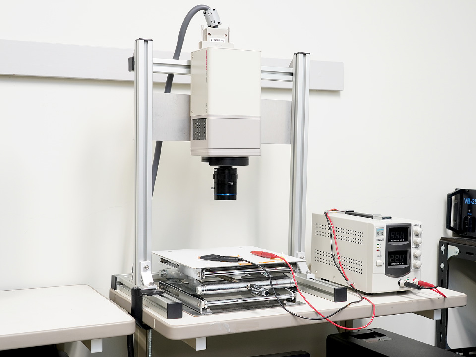
Laser-Beam Induced Current (LBIC) systemChuo Precision Industrial Co., Ltd. and Atto system
The areal distribution of the property of solar cells can be measured by irradiating focused laser light to the solar cell on a laterally-movable X-Y stage.
This system is equipped with three lasers with wavelengths of 470, 653, and 904 nm.
Electroluminescence (EL)Hamamatsu Photonics K.K., C4742-98
Luminescence from a solar cell or a module is captured as an image by applying a forward bias.
The in-plane characteristics of the solar cells can be evaluated.
Solar simulator, external quantum efficiency (EQE)Bunkoukeiki Co.,Ltd., CEP-25
The current–voltage characteristics of solar cells under 1-sun illumination can be measured.
This can also evaluate quantum efficiency, that is, carrier collection probability at each wavelength.
We use this system for the evaluation of solar cells.
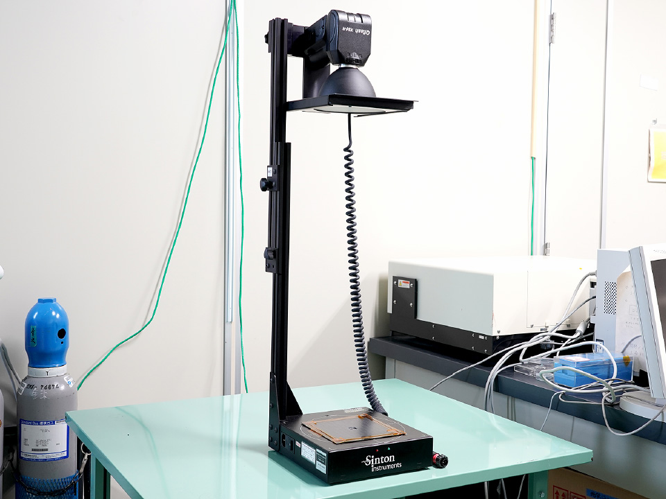
Quasi-steady-state photoconductivity (QSSPC)Sinton Instruments, WCT-120
By measuring the conductivity of crystalline Si during long-duration pulse irradiation which can be considered as steady-state illumination, the effective minority carrier lifetimes of crystalline Si can be measured depending on the density of excess carriers.
We use this system for the quantification of the passivation ability of thin films.
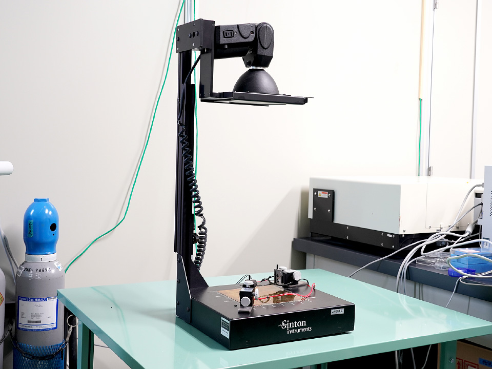
Suns-VocSinton Instruments, Suns-Voc
Quasi current-voltage characteristics can be obtained by measuring the open-circuit voltage (Voc) of a solar cell during long-duration pulse irradiation.
Since there is no current in the circuit, we can obtain a current-voltage characteristics without the effect of series resistance, by which the structure of solar cells can be simplified.
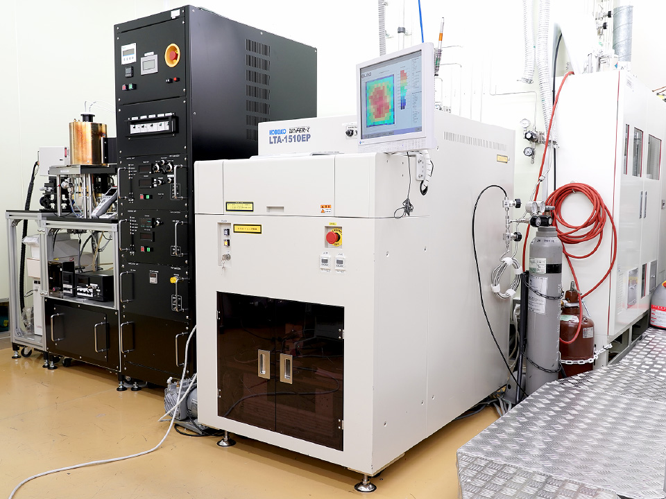
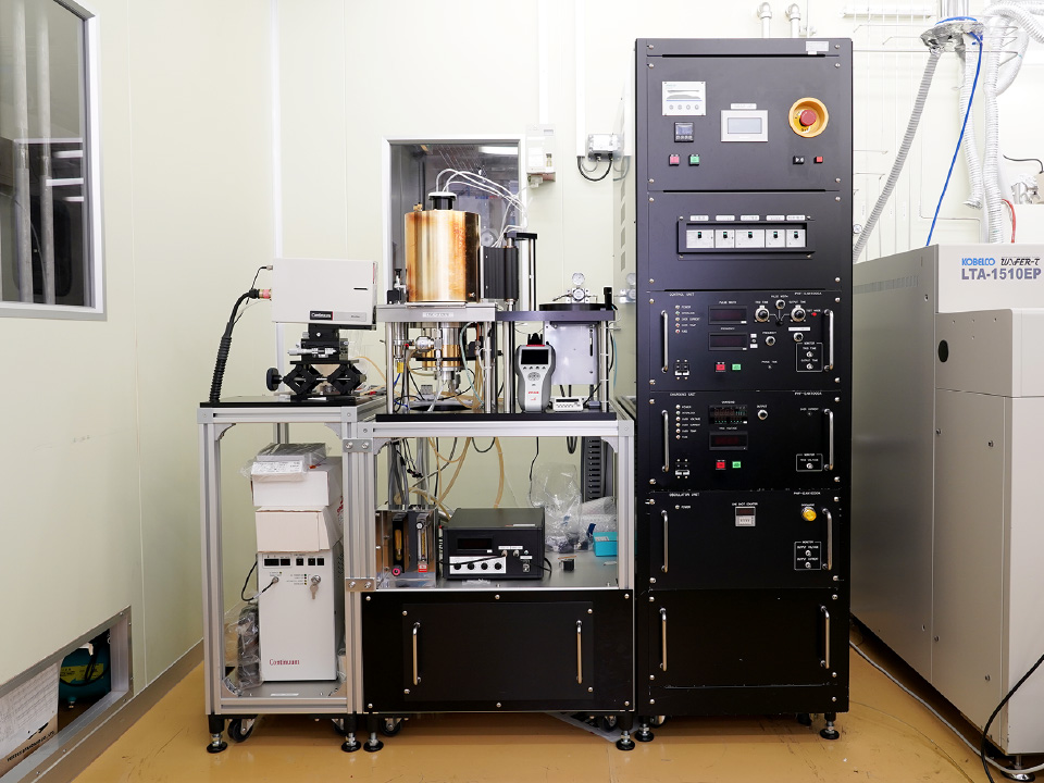
Microwave photoconductivity decay (µ-PCD)Kobelco Research Institute, Inc., LTA-1510EP
This system can observe the recombination of minority carriers in crystalline Si generated by the irradiation of a short-duration pulse and quantify the minority carrier lifetimes of crystalline Si samples by measuring the decay of the reflection intensity of a microwave from a sample.
This system is equipped with two lasers with wavelengths of 904 nm and 349 nm.
Differential µ-PCD measurement is also possible, by which the high-sensitivity measurement for thin films is realized.
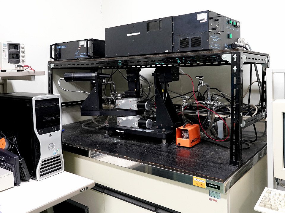
Spectroscopic ellipsometryJ. A. Woolam Japan, WVASE32
The ellipsometry can provide the thickness, refractive index, and dielectric function of thin films by performing an optical model fitting for the intensity and phase differences of s- and p-polarized components of the reflected light for the shallow-angle, linearly-polarized incident light.
We use this for the evaluation of the thicknesses and refractive indices of thin films.
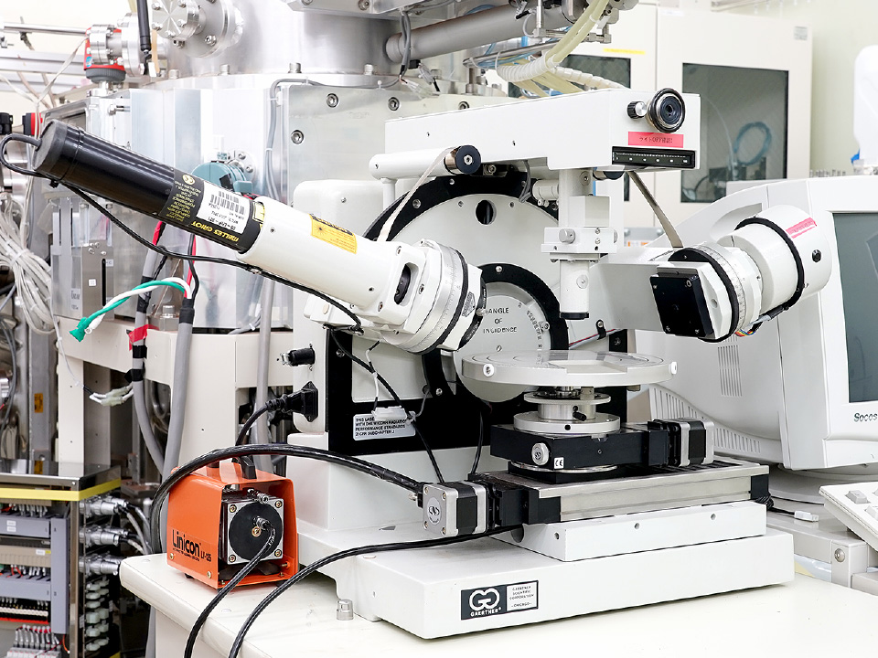
EllipsometryGaertner Scientific Corporation, L115-E
This ellipsometry system, for a single wave measurement using the 632.8 nm line of a He-Ne laser, is equipped with and a mapping function and can evaluate the distribution of the thickness and refractive indices of large-area films.
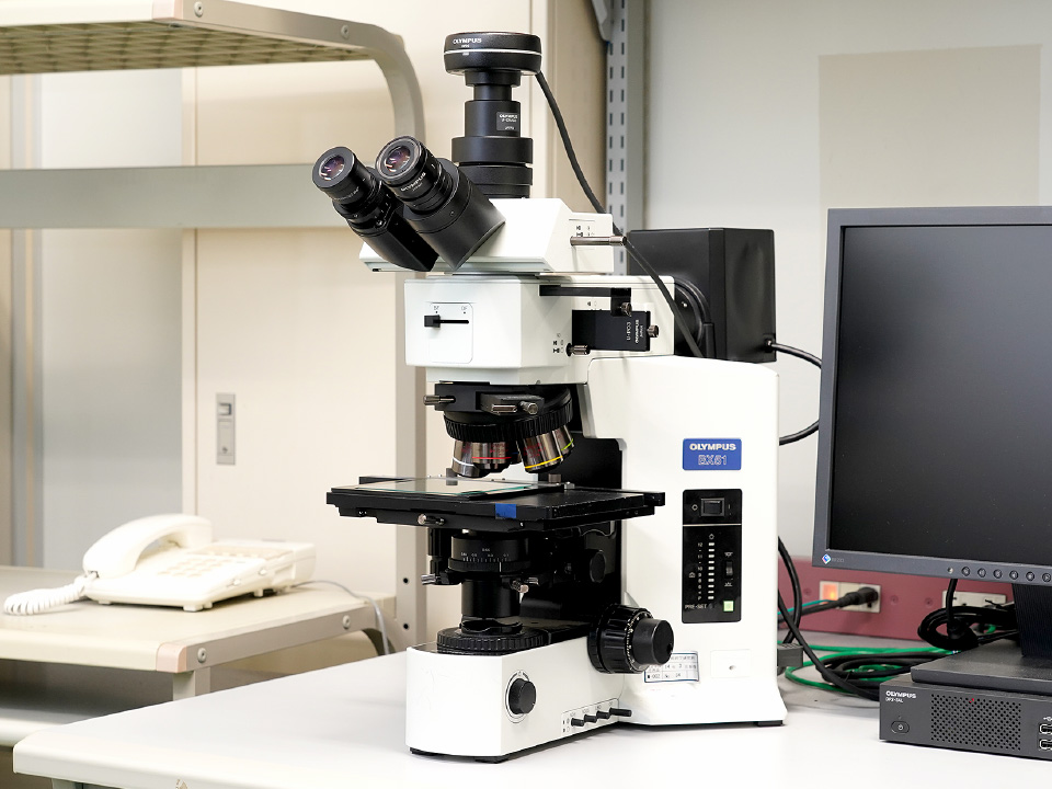
Differential interference contrast microscopeOlympus Corporation, BX51
This optical microscopy can generate images with the information of height by using the difference of the optical path length of two kinds of polarized light.
We use this for the surface observation of thin films.
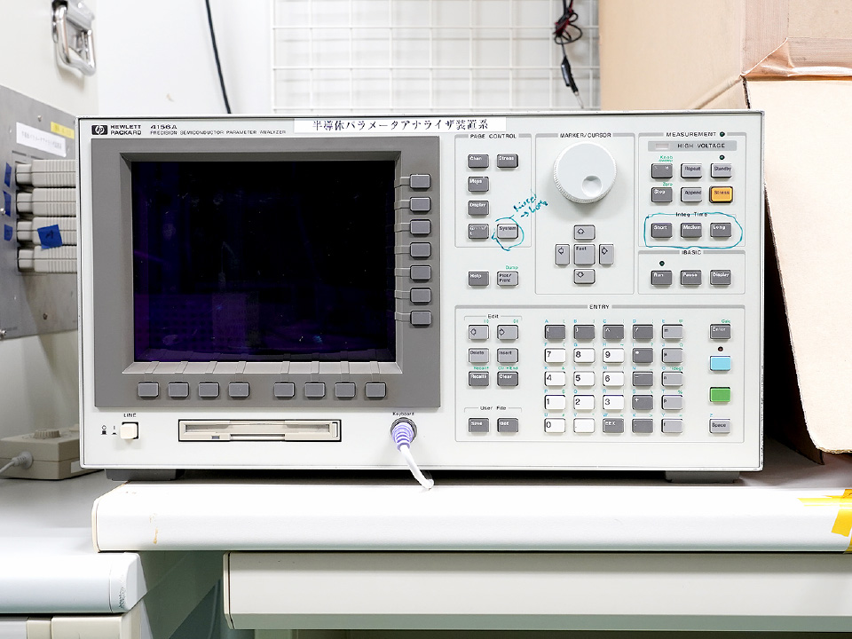
Semiconductor parameter analyzerHewlett Packard, 4156A
This system is used for the evaluation of the current–voltage characteristics of thin films or devices.
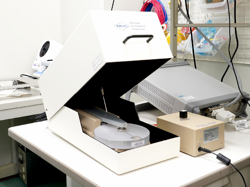
Mercury probeMaterials Development Corporation, 802B-150
Capacitance–voltage characteristics can be measured without forming a surface electrode on a semiconductor.
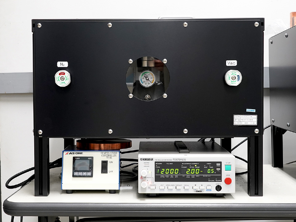
PID test systemTechno Research Ltd.
The PID test of a solar cell can be performed without module fabrication. We can obtain degraded cells by a PID stress, which can be utilized for the surface analysis. This leads to the more detailed clarification of the PID mechanism of photovoltaic modules.