Research
Our group focuses on the following
research topics and attempts to
establish the basic technology of
silicon-based high-performance solar cells.
1. Formation of polycrystalline Si films for solar cells by flash lamp annealing
Thin-film crystalline Si solar cells have been expected as next-generation solar cells due to their advantages such as low amount of material usage and cost-effectiveness. Amorphous Si (a-Si) films on low-cost glass substrates can be crystallized by performing short-duration annealing called flash lamp annealing (FLA), resulting in the formation of poly-Si films. FLA is an annealing method using discharge from a xenon lamp, which is like a flash used for taking photos with a camera but much higher intensity — more than ten thousand of sunlight on the earth. The millisecond-order duration of FLA leads to the thermal diffusion lengths of several tens of µm in glass and a-Si. These allow to prevent thermal damage to entire glass substrates with a thickness of >1 mm and to completely crystallize µm-order-thick a-Si.
FLA induces the lateral crystallization of a-Si films. This lateral crystallization is called explosive crystallization (EC). EC is a domino-like phenomenon. When a-Si (unstable) becomes crystalline Si (stable), the difference of the stability is released as heat. This diffuses into surrounding uncrystallized parts, resulting in further crystallization there. EC is a crystallization driven by the two fundamental processes: heat generation by local crystallization and its diffusion.
There are several types of ECs and their velocities differ depending on the EC modes. The EC of a-Si formed by electron-beam (EB) evaporation proceeds at a velocity of ~14 m/s. This EC is based on liquid-phase epitaxy (LPE), because the EC velocity is in rough agreement with that of LPE at a melting point of a-Si (~1200 °C). The LPE-based EC leads to the formation of poly-Si films consisting of laterally-stretched large grains. On the other hand, a-Si films formed by chemical vapor deposition or sputtering show ECs at a velocity of ~4 m/s. This EC alternates between LPE and solid-phase crystallization at an interval of ~1 µm. Both ECs do not induce the serious diffusion of dopants (boron and phosphorus). This enables to form a crystalline-phase p-n junction just by performing FLA to stacked p-type/n-type a-Si films with keeping their thicknesses and dopant concentrations, resulting in the simple fabrication process of solar cells.
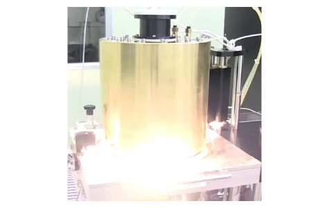
FLA equipment
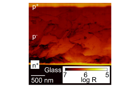
Cross-sectional scanning spreading resistance microscipic (SSRM) image
of a poly-Si film formed from EB-evaporated a-Si by FLA
2. Application of Cat-CVD to the fabrication of solar cells
The suppression of the surface recombination of carriers is essential for high-efficiency crystalline Si solar cells. To suppress the surface recombination, dangling bonds acting as recombination centers must be reduced. The reduction of the number of minority carriers existing near Si surfaces is also effective to mitigate the surface recombination. Thin-film deposition and/or additional doping are thus performed to reduce the surface recombination. However, the surface recombination of carriers is not sufficiently suppressed if damages are induced to crystalline Si during the thin-film deposition or doping.
Plasma-enhanced chemical vapor deposition (PECVD) is the most common method of forming thin films for the production of crystalline Si solar cells. In the PECVD, gas molecules are decomposed through collisions with accelerated electrons, during which charged decomposed species (ions) are formed. The ions gain high kinetic energy by electric field and travel toward crystalline Si, which can induce damages to crystalline Si. The decomposition of gas molecules without ion formation may realize damage-less thin-film formation.
Catalytic chemical vapor deposition (Cat-CVD) is a method of depositing thin films by decomposing gas molecules on a catalyzing wire. Gas molecules are decomposed through two elementary processes: dissociative adsorption and thermal desorption—in other words, catalytic cracking. In the decomposition processes of Cat-CVD, although active decomposed species (radicals) are effectively formed, ions are not generated in principle. Cat-CVD can therefore realize low-damage, “gentle” film formation, which is appropriate for the formation of films aiming at the suppression of carrier recombination on crystalline Si for solar cells.
In addition, Cat-CVD apparatus can be utilized for doping as well as film formation. An ultrathin (~10 nm) doping layer can be formed on a Si surface by exposing Si to decomposed species formed from doping gas (PH3, B2H6). Applying this doping method (Cat-doping) to crystalline Si results in the formation of high-density doping region on the surface, by which the number of minority carriers is reduced and the surface recombination can be suppressed more effectively. Cat-doping is also effective for a-Si, and can thus be utilized for the fabrication of Si heterojunction solar cells.
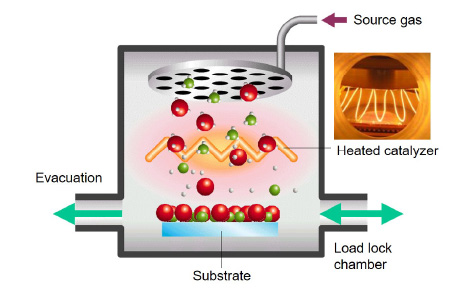
Schematic of Cat-CVD
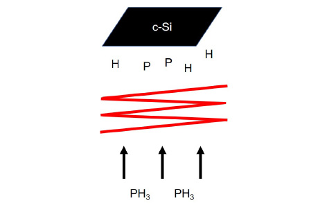
Schematic of Cat-doping
3. Potential-induced degradation of crystalline Si photovoltaic modules
The electricity cost of photovoltaics is determined not only by the fabrication cost and performance of the solar cells and modules. We must consider the ratio of the total generated electricity to the total cost for the installation, maintenance and disposal of the photovoltaic systems. The long-term reliability of the photovoltaic modules is thus important to reduce the cost of photovoltaics.
Recently, potential-induced degradation (PID) has become a significant issue particularly in large-scale photovoltaic power plants. PID is a performance degradation of photovoltaic modules triggered by a voltage between a grounded aluminum frame and cells in a module. For p-type crystalline Si solar cell modules, which has been widely installed so far, their PID phenomena have been considerably clarified and measures against the PID have also been taken. On the other hand, for n-type crystalline Si solar cell modules, which will increase their market share in the near future due to their better performance than p-type ones, their PID has not been fully investigated. Furthermore, there are a plenty of cell structures in n-type wafer-based solar cells. For example, there are several possibility of the location of a p-n junction in the cell, and some solar cells have a heterojunction consisting of a-Si and crystalline Si. Cells with different structures show different PID behaviors under different mechanisms.
There are mainly two causes of the PID of crystalline Si photovoltaic modules. One is the accumulation of charges in Si nitride, leading to an increase in the number of minority carrier near the Si surface and an enhancement in surface recombination. The other is the introduction of impurities, such as sodium (Na), driven from the cover glass of the modules by an electric field, by which current paths penetrating the p-n junction are formed and/or carrier recombination is enhanced. The presence or absence and the degree of these degradations differs depending on the structure of the cells, and the PID of the n-type crystalline Si photovoltaic modules muse be investigated for each cell structure. In addition, since the PID of the outdoor modules always occurs under the sunlight illumination, the effects of light irradiation on the PID should also be clarified.
For the investigation of the PID of crystalline Si photovoltaic modules, commercialized large-size photovoltaic modules are not necessary, and small-sized modules with a 2×2 cm2-sized cell can reproduce the outdoor PID. We also have a PID test system for unencapsulated cells. This equipment enables us to obtain degraded cells themselves, which can be utilized for experiments such as elemental analysis.
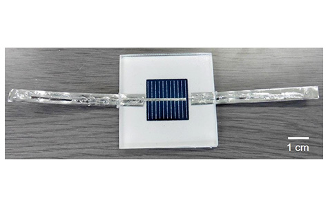
Small Si photovoltaic module for a PID test
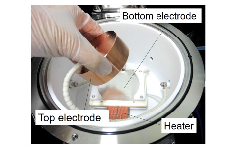
PID-test chamber for unencapsulated cells